NAND512R3A2CZA6E
| Part Description |
IC FLASH 512MBIT PAR 63VFBGA |
|---|---|
| Quantity | 272 Available (as of June 14, 2026) |

| Product Category | Memory |
|---|---|
| Manufacturer | Micron Technology Inc. |
| Manufacturing Status | Obsolete |
| Manufacturer Standard Lead Time | Contact Us |
| Datasheet |
Specifications & Environmental
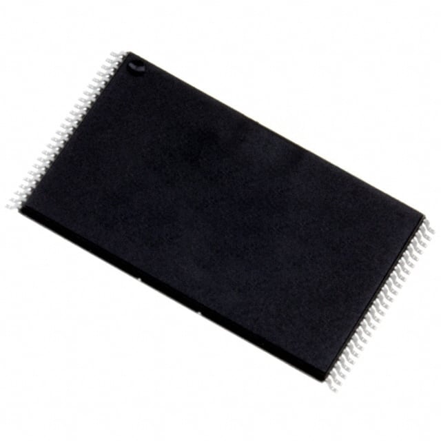
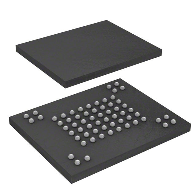
| Device Package | 63-VFBGA (9x11) | Memory Format | FLASH | Technology | FLASH - NAND | ||
|---|---|---|---|---|---|---|---|
| Memory Size | 512 Mbit | Access Time | 50 ns | Grade | Industrial | ||
| Clock Frequency | N/A | Voltage | 1.7V ~ 1.95V | Memory Type | Non-Volatile | ||
| Operating Temperature | -40°C ~ 85°C (TA) | Write Cycle Time Word Page | 50 ns | Packaging | 63-TFBGA | ||
| Mounting Method | Non-Volatile | Memory Interface | Parallel | Memory Organization | 64M x 8 | ||
| Moisture Sensitivity Level | 3 (168 Hours) | RoHS Compliance | ROHS3 Compliant | REACH Compliance | REACH Unaffected | ||
| Qualification | N/A | ECCN | 3A991B1A | HTS Code | 8542.32.0071 |
Overview of NAND512R3A2CZA6E – IC FLASH 512MBIT PAR 63VFBGA
The NAND512R3A2CZA6E is a 512‑Mbit SLC NAND flash memory organized as 64M × 8 with a parallel interface. It provides page‑oriented NAND architecture (528‑byte page for x8), designed for cost‑effective mass storage applications.
Key hardware attributes include low‑voltage operation (1.7 V–1.95 V), fast access characteristics (50 ns typical sequential access), industrial operating range (‑40 °C to 85 °C), and a 63‑ball VFBGA package (9 × 11 mm footprint).
Key Features
- Memory Core 512 Mbit SLC NAND organized as 64M × 8 with 528‑byte page structure (x8 device: 512 + 16 spare bytes).
- Performance Page and random access optimized for NAND workflows — sequential access down to 50 ns (1.8 V) and random page access timing per device specifications.
- Power Low‑voltage supply range of 1.7 V to 1.95 V suitable for 1.8 V system domains.
- Endurance & Retention Program/erase endurance characterized at 100,000 cycles (with ECC) and data retention specified at 10 years.
- Interface & Organization Parallel NAND interface with multiplexed address/data bus and support for standard NAND command set and operations (page program, copy‑back, block erase).
- Reliability & Data Protection Built‑in features include status register, hardware data protection (program/erase lock during power transitions), bad block management support and ECC models referenced in documentation.
- Package & Temperature 63‑VFBGA package (9 × 11 × 1.05 mm typical) and operating temperature range of ‑40 °C to 85 °C (TA).
- Security & Factory Options Includes OTP area, serial number (unique ID) option, and security feature fields described in the device specification.
- Development Resources Documentation and development assets include ECC models, wear‑leveling and bad‑block management guidance and hardware simulation models cited in the datasheet.
Typical Applications
- Mass Storage Systems Suited for cost‑sensitive mass storage applications requiring a parallel NAND flash element and SLC endurance characteristics.
- Embedded Storage Firmware and file storage in embedded devices that need compact, non‑volatile parallel NAND with spare‑area support for metadata and ECC.
- Industrial Equipment Designs operating across an extended temperature range (‑40 °C to 85 °C) that require non‑volatile NAND storage with high program/erase endurance.
Unique Advantages
- High‑density SLC NAND: 512 Mbit capacity in a compact BGA package enables larger on‑board storage without external memory stacks.
- Low‑voltage operation: 1.7 V–1.95 V supply range supports integration into 1.8 V system domains for reduced power rail complexity.
- Proven endurance and retention: 100,000 program/erase cycles (with ECC) and 10 years data retention help assure long operational life for fielded products.
- Parallel NAND interface: Standard NAND command/data/addr multiplexing simplifies controller integration for existing parallel NAND ecosystems.
- Compact BGA package: 63‑VFBGA (9 × 11 mm) provides small footprint mounting for space‑constrained board designs.
- Documented system support: Datasheet includes ECC models, wear‑leveling and bad‑block management guidance and simulation models to accelerate development and validation.
Why Choose NAND512R3A2CZA6E?
The NAND512R3A2CZA6E positions as a practical SLC NAND flash building block for designs that need a balance of density, endurance and low‑voltage operation. Its 64M × 8 organization, robust program/erase cycle characterization, and spare‑area layout make it suitable for storage systems that require predictable NAND behavior and data integrity features.
This device is appropriate for engineers implementing embedded and industrial storage solutions where compact BGA packaging, extended temperature range and available software/hardware guidance (ECC, wear leveling, bad block management) reduce integration risk and speed time to market.
Request a quote or submit an inquiry to receive pricing and availability information for NAND512R3A2CZA6E.