
NAND512R3A2BZA6E
| Part Description |
IC FLASH 512MBIT PAR 63VFBGA |
|---|---|
| Quantity | 1,424 Available (as of June 14, 2026) |

| Product Category | Memory |
|---|---|
| Manufacturer | STMicroelectronics |
| Manufacturing Status | Obsolete |
| Manufacturer Standard Lead Time | Contact Us |
| Datasheet |
Specifications & Environmental
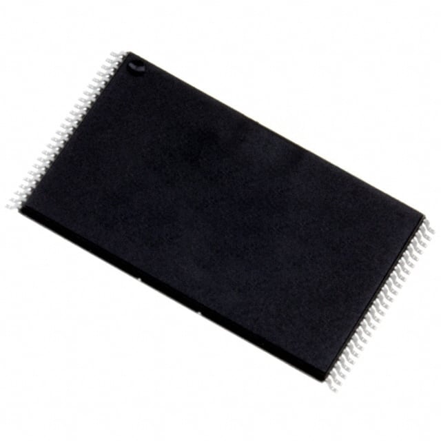
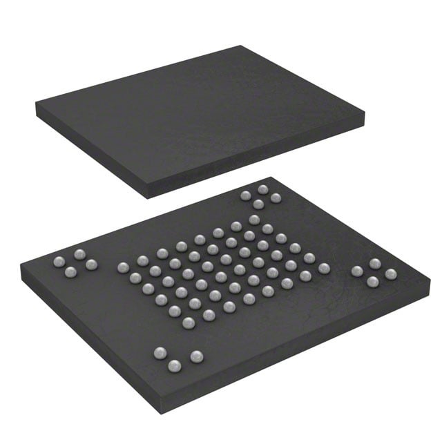
| Device Package | 63-VFBGA (8.5x15) | Memory Format | FLASH | Technology | FLASH - NAND | ||
|---|---|---|---|---|---|---|---|
| Memory Size | 512 Mbit | Access Time | 60 ns | Grade | Industrial | ||
| Clock Frequency | N/A | Voltage | 1.7V ~ 1.95V | Memory Type | Non-Volatile | ||
| Operating Temperature | -40°C ~ 85°C (TA) | Write Cycle Time Word Page | 60 ns | Packaging | 63-VFBGA | ||
| Mounting Method | Non-Volatile | Memory Interface | Parallel | Memory Organization | 64M x 8 | ||
| Moisture Sensitivity Level | 3 (168 Hours) | RoHS Compliance | ROHS3 Compliant | REACH Compliance | REACH Unaffected | ||
| Qualification | N/A | ECCN | 3A991B1A | HTS Code | 8542.32.0071 |
Overview of NAND512R3A2BZA6E – 512 Mbit Parallel NAND Flash, 63-VFBGA
The NAND512R3A2BZA6E is a 512 Mbit non-volatile NAND Flash memory organized as 64M × 8. It implements a parallel NAND interface in a 63‑VFBGA (8.5 × 15 mm) package and is designed for mass-storage and embedded boot applications that require high-density non-volatile storage.
With a 1.7 V to 1.95 V supply range, industrial operating temperature support (‑40 °C to 85 °C), and on-chip NAND features such as automatic page 0 read and status register, this device targets embedded systems that need compact, low‑voltage flash storage with development tool support for error correction and bad-block management.
Key Features
- Memory Architecture — 512 Mbit NAND Flash organized as 64M × 8 with parallel x8 bus width.
- High Density Storage — Designed as a high-density NAND family member (128 Mbit to 1 Gbit); cost-effective solution for mass storage applications as described in the product family summary.
- Page and Block Structure — x8 page size defined as 528 bytes (512 + 16 spare) and block sizes consistent with the NAND family (x8 block: 16K + 512 spare bytes); supports page program and block erase operations.
- Read/Program/Erase Performance — Access time specified at 60 ns with write cycle time (word/page) at 60 ns; datasheet extracts report page program time (typical 200 μs) and block erase time (typical 2 ms).
- Low-Voltage Operation — 1.8 V device operation with VDD = 1.7 to 1.95 V for lower-power system designs.
- Reliability and Data Integrity — On‑chip hardware data protection during power transitions; rated for 100,000 program/erase cycles and 10 years data retention according to the product family documentation.
- System-Level Features — NAND interface with multiplexed address/data lines, copy-back program mode for internal page-to-page copies without external buffering, status register and electronic signature, and an automatic page‑0 read at power‑up option for boot support.
- Package and Temperature — 63‑VFBGA package (8.5 × 15 mm) with operating temperature range from ‑40 °C to 85 °C.
- Development Support — Family documentation and tools include ECC software/hardware models, bad-block management and wear-leveling algorithms, and reference/demo software and boards as noted in the product materials.
Typical Applications
- Mass Storage — High-density NAND array suitable for embedded mass-storage use where compact non-volatile capacity is required.
- Embedded Boot Memory — Automatic page‑0 read at power-up and electronic signature features enable boot and automatic memory download scenarios.
- Consumer and Portable Devices — Compact 63‑VFBGA package and low-voltage (1.7–1.95 V) operation fit space‑constrained, battery‑operated designs requiring solid-state storage.
Unique Advantages
- High-density, parallel NAND array: 512 Mbit capacity in a single x8 device simplifies board design for medium-density storage requirements.
- Low-voltage operation: 1.7 V to 1.95 V VDD range enables lower power supply design choices and compatibility with 1.8 V systems.
- Built-in storage management features: Copy-back program mode, status register, electronic signature and automatic page‑0 read reduce external buffering and simplify boot flows.
- Robust data endurance and retention: Product family specifies 100,000 program/erase cycles and 10 years data retention for lifecycle planning.
- Compact BGA footprint: 63‑VFBGA (8.5 × 15 mm) provides a small board area for systems where PCB space is constrained.
- Development and integration support: Family-level ECC models, bad-block management, and reference software/boards help accelerate integration and validation.
Why Choose IC FLASH 512MBIT PAR 63VFBGA?
The IC FLASH 512MBIT PAR 63VFBGA (NAND512R3A2BZA6E) offers a straightforward, parallel x8 NAND Flash option for designs that need 512 Mbit of non-volatile storage in a compact BGA package. Its low-voltage VDD range, on-chip NAND management features, and documented endurance/retention characteristics make it suitable for embedded mass-storage and boot memory applications.
Engineers designing space- and power-constrained systems will find the device’s package, supply requirements, and available development resources (ECC and bad-block management models, demo boards, and reference software) helpful for speeding integration and validation in production designs.
Request a quote or submit a purchase inquiry to receive pricing and availability information for NAND512R3A2BZA6E.


Date Founded: 1987
Headquarters: Plan-les-Ouates, Geneva, Switzerland
Employees: 50,000+
Revenue: $17.24 Billion
Certifications and Memberships: ISO9001:2015, ISO14001:2015, ISO45001:2018, IATF16949:2016, ISO50001:2018


