
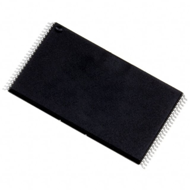
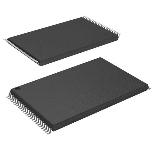
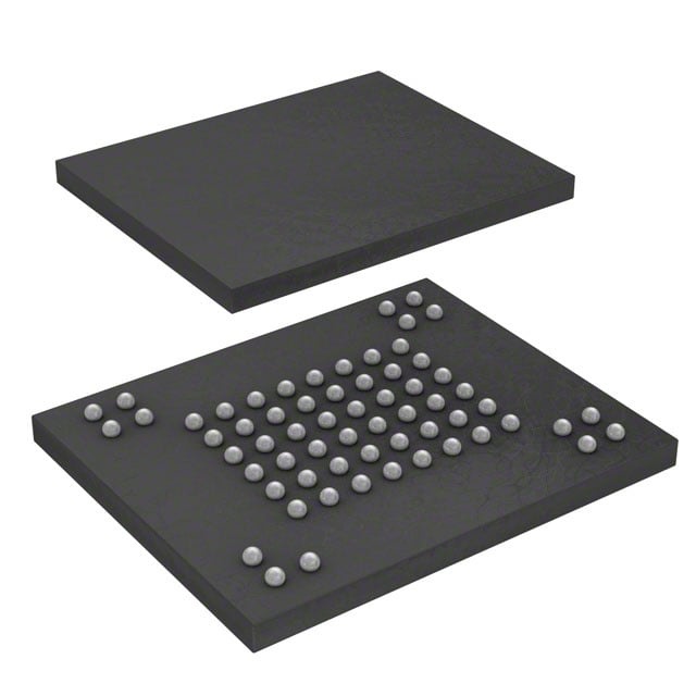
NAND512R3A2AZA6E
| Part Description |
IC FLASH 512MBIT PAR 55VFBGA |
|---|---|
| Quantity | 352 Available (as of June 14, 2026) |

| Product Category | Memory |
|---|---|
| Manufacturer | STMicroelectronics |
| Manufacturing Status | Obsolete |
| Manufacturer Standard Lead Time | Contact Us |
| Datasheet |
Specifications & Environmental
| Device Package | 55-VFBGA (8x10) | Memory Format | FLASH | Technology | FLASH - NAND | ||
|---|---|---|---|---|---|---|---|
| Memory Size | 512 Mbit | Access Time | 60 ns | Grade | Industrial | ||
| Clock Frequency | N/A | Voltage | 1.7V ~ 1.95V | Memory Type | Non-Volatile | ||
| Operating Temperature | -40°C ~ 85°C (TA) | Write Cycle Time Word Page | 60 ns | Packaging | 55-TFBGA | ||
| Mounting Method | Non-Volatile | Memory Interface | Parallel | Memory Organization | 64M x 8 | ||
| Moisture Sensitivity Level | 1 (Unlimited) | RoHS Compliance | RoHS non-compliant | REACH Compliance | REACH Unaffected | ||
| Qualification | N/A | ECCN | 3A991B1A | HTS Code | 8542.32.0071 |
Overview of NAND512R3A2AZA6E – IC FLASH 512MBIT PAR 55VFBGA
The NAND512R3A2AZA6E is a 512 Mbit parallel NAND Flash memory device in a 55-ball VFBGA/TFBGA package. It implements NAND architecture (64M × 8 organization) and is intended for mass storage and embedded flash applications where non-volatile, high-density storage is required.
Designed for low-voltage 1.8V systems, the device delivers block- and page-level operations with features for boot support, hardware data protection and development tools for error correction and bad-block management.
Key Features
- Memory Type & Capacity 512 Mbit NAND Flash memory organized as 64M × 8 for parallel x8 operation.
- Interface Parallel NAND interface (x8); the device family supports x8 or x16 bus widths with pinout compatibility across densities.
- Low-Voltage Supply 1.8V device operation with VDD range from 1.7V to 1.95V suitable for low-voltage systems.
- Performance Characteristics Specified access time of 60 ns with write/word page cycle time of 60 ns. Datasheet values include page program typical time of 200 μs, block erase typical time of 2 ms, random page read up to 12 μs and sequential access as low as 50 ns.
- Package Options Available in compact 55-ball FBGA formats (55-TFBGA / 55-VFBGA, 8 × 10 mm) for space-constrained board designs.
- Operational Temperature Specified operating ambient range from −40°C to +85°C.
- Data Integrity & Durability Designed for endurance with 100,000 program/erase cycles and typical data retention of 10 years.
- Boot & System Support Options include automatic page 0 read at power-up to support boot-from-NAND and automatic memory download functionality.
- Protection & Management Hardware data protection during power transitions plus support resources for ECC, bad-block management and wear-leveling algorithms.
Typical Applications
- Mass storage devices High-density NAND for embedded storage and removable media controllers where non-volatile block storage is required.
- System boot memory Automatic page 0 read at power-up enables use as boot memory in embedded systems.
- Consumer and industrial electronics Compact FBGA package and low-voltage operation fit space- and power-constrained designs in consumer and industrial products.
Unique Advantages
- High-density storage in a compact package: 512 Mbit capacity in a 55-ball FBGA (8 × 10 mm) minimizes board area for high-capacity designs.
- Low-voltage operation: 1.7–1.95V supply range supports modern 1.8V power rails for reduced system power consumption.
- Fast page and block operations: Page program, block erase and read timing figures (typical and maximum as provided) enable responsive block-level storage operations.
- System-level boot support: Automatic page 0 read at power-up simplifies system boot designs that load firmware from NAND.
- Design and reliability support: Built-in hardware protection, standard ECC/bad-block management guidance and development tools help accelerate integration and improve field reliability.
- Family scalability: Part of a NAND family with up to 1 Gbit densities and pinout compatibility across densities for design scalability.
Why Choose NAND512R3A2AZA6E?
NAND512R3A2AZA6E provides a balanced combination of density, low-voltage operation and system-oriented features such as automatic power-up page read and hardware data protection. Its FBGA 55-ball package and 64M × 8 organization make it suitable for embedded storage and boot applications where board space and power are constrained.
This device is appropriate for engineers specifying NAND Flash for mass storage or embedded boot tasks who require clear program/erase endurance figures, development support for ECC and bad-block management, and compatibility within a broader family of NAND densities for future scaling.
Request a quote or contact sales to discuss availability, lead times and volume pricing for NAND512R3A2AZA6E.


Date Founded: 1987
Headquarters: Plan-les-Ouates, Geneva, Switzerland
Employees: 50,000+
Revenue: $17.24 Billion
Certifications and Memberships: ISO9001:2015, ISO14001:2015, ISO45001:2018, IATF16949:2016, ISO50001:2018


