
NAND512W3A0AN6E
| Part Description |
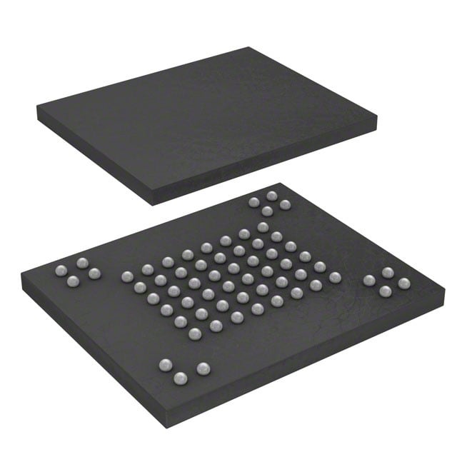
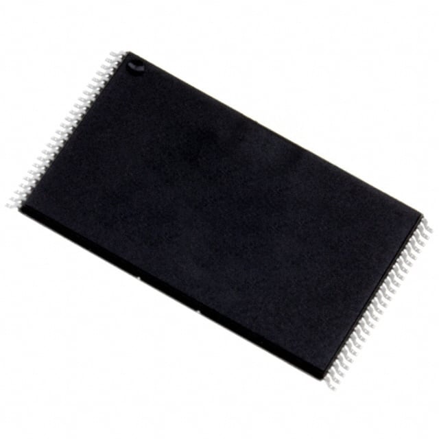
IC FLASH 512MBIT PARALLEL 48TSOP |
|---|---|
| Quantity | 593 Available (as of June 15, 2026) |

| Product Category | Memory |
|---|---|
| Manufacturer | STMicroelectronics |
| Manufacturing Status | Obsolete |
| Manufacturer Standard Lead Time | Contact Us |
| Datasheet |
Specifications & Environmental
| Device Package | 48-TSOP | Memory Format | FLASH | Technology | FLASH - NAND | ||
|---|---|---|---|---|---|---|---|
| Memory Size | 512 Mbit | Access Time | 50 ns | Grade | Industrial | ||
| Clock Frequency | N/A | Voltage | 2.7V ~ 3.6V | Memory Type | Non-Volatile | ||
| Operating Temperature | -40°C ~ 85°C (TA) | Write Cycle Time Word Page | 50 ns | Packaging | 48-TFSOP (0.724", 18.40mm Width) | ||
| Mounting Method | Non-Volatile | Memory Interface | Parallel | Memory Organization | 64M x 8 | ||
| Moisture Sensitivity Level | 1 (Unlimited) | RoHS Compliance | RoHS non-compliant | REACH Compliance | REACH Unaffected | ||
| Qualification | N/A | ECCN | 3A991B1A | HTS Code | 8542.32.0071 |
Overview of NAND512W3A0AN6E – IC FLASH 512MBIT PARALLEL 48TSOP
The NAND512W3A0AN6E is a 512 Mbit non-volatile NAND flash memory organized as 64M × 8 with a parallel NAND interface in a 48‑TSOP package. It targets mass storage and embedded boot/firmware applications where high density, NAND architecture and a standard TSOP48 footprint are required.
Built for 3.0V systems (VDD = 2.7 V to 3.6 V) and rated for industrial operating temperatures (−40 °C to 85 °C), the device provides page-level read/program operations, block erase, and on‑chip features to support system boot and data integrity.
Key Features
- Memory Core — 512 Mbit NAND flash organized as 64M × 8 with x8 bus width and parallel NAND interface.
- Page and Block Architecture — x8 device page size: 512 + 16 spare bytes; block size: 16K + 512 spare bytes, suitable for typical NAND mass storage layouts.
- Read / Program / Erase Performance — Random page read up to 12 μs (max), sequential access 50 ns (min); typical page program time ~200 μs and typical block erase time ~2 ms.
- Endurance & Data Retention — Specified for 100,000 program/erase cycles and 10 years data retention.
- Power and Timing — Supply voltage 2.7 V to 3.6 V; listed access and write cycle timing includes 50 ns values for sequential access and write cycle time (word/page).
- On‑chip Functionality — Features include copy‑back program mode, status register, electronic signature, chip‑enable “don’t care” option, and automatic page‑0 read at power‑up for boot support.
- System Reliability — Hardware data protection locks program/erase during power transitions; includes support for ECC, bad block management and wear leveling in provided development toolset.
- Package and Temperature — 48‑TSOP (48‑TFSOP / 48‑TSOP footprint) package; operating range −40 °C to 85 °C.
Typical Applications
- Mass Storage Applications — High‑density NAND for file and data storage in cost‑sensitive embedded products.
- Embedded Boot / Firmware Storage — Automatic page‑0 read at power‑up enables direct boot and automatic memory download for firmware devices.
- Portable and Consumer Devices — Non‑volatile program and data storage where compact TSOP48 packaging and 3.0V supply compatibility are required.
- Development and Evaluation — Supported by ECC models, bad block management, wear leveling algorithms and PC demo boards for software and hardware development.
Unique Advantages
- High Density in Standard Footprint: 512 Mbit capacity in a 48‑TSOP package provides large storage without unconventional packaging.
- Boot‑Ready Behavior: Automatic page‑0 read at power‑up simplifies system boot and firmware download flows.
- Proven NAND Feature Set: Copy‑back program, status register and electronic signature facilitate efficient block/page management and system integration.
- Robust Data Integrity: 100,000 P/E cycles and 10‑year retention combined with hardware protection during power transitions support long term reliability.
- Design and Development Support: Provided ECC software/hardware models and bad block/wear leveling algorithms help accelerate integration and validation.
- Wide 3.0V Compatibility: Operates across 2.7 V to 3.6 V supplies to match common 3.0V embedded system rails.
Why Choose NAND512W3A0AN6E?
The NAND512W3A0AN6E delivers a balanced combination of density, standard packaging and NAND feature set geared toward mass storage and embedded boot/firmware applications. Its x8 NAND organization, page/block architecture and on‑chip behaviors (including automatic page‑0 read and copy‑back) make it suitable for systems that require direct boot capability and efficient page/block operations.
With industrial temperature range, a broad 3.0V supply window, endurance and retention specifications, and available development tools for ECC and block management, the device is positioned for designers seeking a reliable NAND solution that integrates into standard TSOP48 footprints and supported development ecosystems.
Request a quote or submit an inquiry to obtain pricing, availability and lead‑time information for the NAND512W3A0AN6E.


Date Founded: 1987
Headquarters: Plan-les-Ouates, Geneva, Switzerland
Employees: 50,000+
Revenue: $17.24 Billion
Certifications and Memberships: ISO9001:2015, ISO14001:2015, ISO45001:2018, IATF16949:2016, ISO50001:2018


