
NAND512W3A2BN6E
| Part Description |
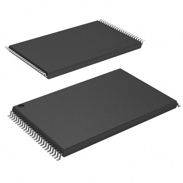
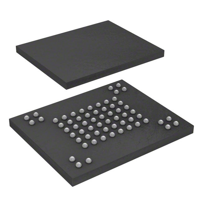
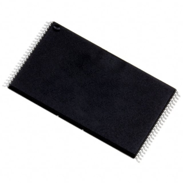
IC FLASH 512MBIT PARALLEL 48TSOP |
|---|---|
| Quantity | 591 Available (as of June 14, 2026) |

| Product Category | Memory |
|---|---|
| Manufacturer | STMicroelectronics |
| Manufacturing Status | Obsolete |
| Manufacturer Standard Lead Time | Contact Us |
| Datasheet |
Specifications & Environmental
| Device Package | 48-TSOP | Memory Format | FLASH | Technology | FLASH - NAND | ||
|---|---|---|---|---|---|---|---|
| Memory Size | 512 Mbit | Access Time | 50 ns | Grade | Industrial | ||
| Clock Frequency | N/A | Voltage | 2.7V ~ 3.6V | Memory Type | Non-Volatile | ||
| Operating Temperature | -40°C ~ 85°C (TA) | Write Cycle Time Word Page | 50 ns | Packaging | 48-TFSOP (0.724", 18.40mm Width) | ||
| Mounting Method | Non-Volatile | Memory Interface | Parallel | Memory Organization | 64M x 8 | ||
| Moisture Sensitivity Level | 3 (168 Hours) | RoHS Compliance | ROHS3 Compliant | REACH Compliance | REACH Unaffected | ||
| Qualification | N/A | ECCN | 3A991B1A | HTS Code | 8542.32.0071 |
Overview of NAND512W3A2BN6E – IC FLASH 512MBIT PARALLEL 48TSOP
The NAND512W3A2BN6E is a 512 Mbit parallel NAND flash memory organized as 64M x 8. It implements a high-density NAND Flash architecture with a parallel x8 interface suited for mass storage and embedded boot/firmware applications.
Designed for 3.0V systems (VDD 2.7V to 3.6V) and extended temperature operation (–40°C to 85°C), the device balances storage density, access performance, and system-level features such as automatic page read at power-up and hardware data protection.
Key Features
- Core / Memory: 512 Mbit NAND Flash organized as 64M x 8, providing a high-density non-volatile memory array for mass storage and firmware.
- Page and Block Geometry: x8 device page size is 512 + 16 spare bytes and block size is 16K + 512 spare bytes, enabling standard NAND page/block management.
- Performance: Random page read up to 12 µs (max), sequential access 50 ns (min), page program time ~200 µs (typ), and block erase time ~2 ms (typ).
- Interface: Parallel NAND interface with multiplexed address/data lines and pinout compatibility across densities for design flexibility.
- Power: Supported supply voltage range 2.7 V to 3.6 V (3.0V device range).
- Reliability & Endurance: Data retention specified at 10 years and program/erase endurance of 100,000 cycles.
- System-level Features: Copy-back program mode for fast page-to-page copy without external buffering, status register, electronic signature, and automatic page 0 read at power-up (boot support).
- Protection: Hardware data protection that locks program/erase operations during power transitions.
- Package & Temperature: 48-TSOP package (48-TFSOP, 0.724" / 18.40 mm width) rated for –40°C to 85°C ambient.
- Development Support: Provided error correction code (ECC) models, bad block management and wear-leveling algorithms, and demo/utility resources for integration.
Typical Applications
- Mass Storage Systems — High-density NAND array and spare area support cost-effective file storage and large-volume data retention.
- Embedded Boot and Firmware Storage — Automatic page 0 read at power-up enables boot-from-NAND and automatic memory download scenarios.
- Consumer and Portable Devices — Parallel x8 interface and compact 48-TSOP package simplify integration into compact embedded designs.
- Data Logging and Firmware Update Storage — Endurance (100,000 P/E cycles) and 10-year data retention accommodate long-term firmware and log storage needs.
Unique Advantages
- High-density, x8 NAND Array: 512 Mbit capacity in a 64M x 8 organization provides substantial non-volatile storage without additional devices.
- Comprehensive Page/Block Geometry: Standard 512+16 spare byte pages and 16K+512 spare byte blocks simplify established NAND management schemes.
- Boot and System Utilities: Automatic page 0 read at power-up and copy-back program mode reduce external buffering and simplify bootload and in-system data moves.
- Robust Endurance and Retention: 100,000 program/erase cycles and 10 years data retention support reliable long-term storage.
- Wide Supply and Temperature Range: Operation from 2.7 V to 3.6 V and –40°C to 85°C ambient addresses a broad set of embedded and industrial environments.
- Design and Integration Support: ECC models, bad block management, wear-leveling algorithms, and demo resources aid integration and reduce development time.
Why Choose NAND512W3A2BN6E?
NAND512W3A2BN6E positions itself as a practical high-density parallel NAND Flash option for designers needing 512 Mbit of non-volatile storage with established NAND page/block geometries and system-level features such as automatic power-up page read and copy-back programming. Its combination of endurance, retention, and development resources makes it suitable for embedded storage, boot memory, and mass storage designs that require proven NAND management.
This device is well suited to engineers and procurement teams targeting scalable storage capacity in a compact 48-TSOP package, across a 2.7–3.6 V supply range and an industrial temperature window, while leveraging available ECC and wear-leveling tools for integration.
Request a quote or submit a pricing inquiry to check availability and discuss how NAND512W3A2BN6E can meet your storage and boot-memory requirements.


Date Founded: 1987
Headquarters: Plan-les-Ouates, Geneva, Switzerland
Employees: 50,000+
Revenue: $17.24 Billion
Certifications and Memberships: ISO9001:2015, ISO14001:2015, ISO45001:2018, IATF16949:2016, ISO50001:2018


