NAND512W3A2CN6E
| Part Description |
IC FLASH 512MBIT PARALLEL 48TSOP |
|---|---|
| Quantity | 1,130 Available (as of June 11, 2026) |
| Product Category | Memory |
|---|---|
| Manufacturer | Micron Technology Inc. |
| Manufacturing Status | Obsolete |
| Manufacturer Standard Lead Time | Contact Us |
| Datasheet |
Specifications & Environmental
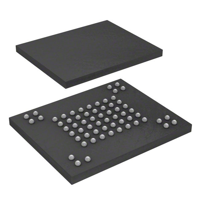
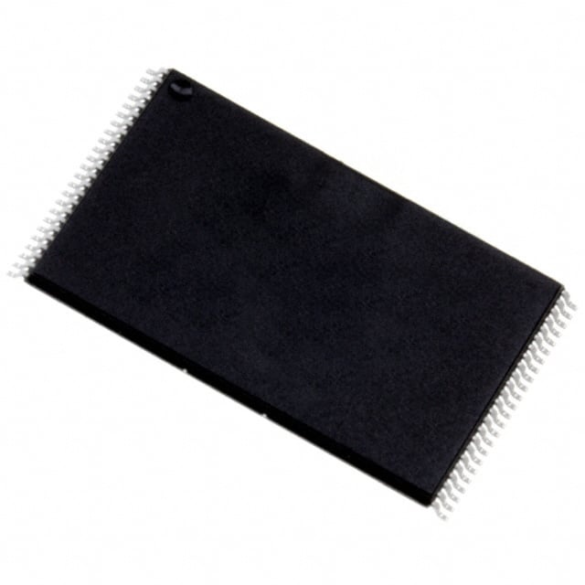
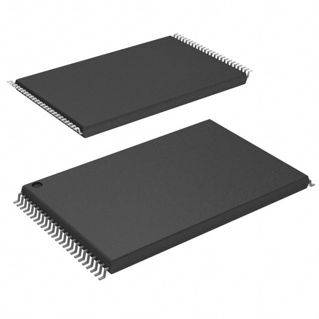
| Device Package | 48-TSOP | Memory Format | FLASH | Technology | FLASH - NAND | ||
|---|---|---|---|---|---|---|---|
| Memory Size | 512 Mbit | Access Time | 50 ns | Grade | Industrial | ||
| Clock Frequency | N/A | Voltage | 2.7V ~ 3.6V | Memory Type | Non-Volatile | ||
| Operating Temperature | -40°C ~ 85°C (TA) | Write Cycle Time Word Page | 50 ns | Packaging | 48-TFSOP (0.724", 18.40mm Width) | ||
| Mounting Method | Non-Volatile | Memory Interface | Parallel | Memory Organization | 64M x 8 | ||
| Moisture Sensitivity Level | 3 (168 Hours) | RoHS Compliance | ROHS Compliant | REACH Compliance | REACH Unaffected | ||
| Qualification | N/A | ECCN | 3A991B1A | HTS Code | 8542.32.0071 |
Overview of NAND512W3A2CN6E – IC FLASH 512MBIT PARALLEL 48TSOP
The NAND512W3A2CN6E is a 512 Mbit parallel NAND flash memory device in a 48-TSOP package. It implements SLC NAND flash architecture with a parallel NAND interface and is targeted at high-density mass storage and embedded memory applications.
Designed for integration where non-volatile, board-mounted storage is required, the device combines page-based organization, fast access characteristics, and industry-standard signaling for streamlined system integration.
Key Features
- Memory Capacity & Organization — 512 Mbit total capacity organized as 64M x 8 with a page architecture of 528-byte / 264-word pages (x8/x16 distinction noted in datasheet).
- Parallel NAND Interface — Standard NAND interface with x8 bus width, multiplexed address/data lines and support for common NAND command and control signals for direct host/controller interfacing.
- Performance — Access time specified at 50 ns; datasheet lists random and sequential read characteristics and a typical page program time of 200 μs and typical fast block erase time of 2 ms.
- Write/Read Timing — Write cycle time (word/page) listed at 50 ns; datasheet provides random access (12 μs @ 3 V / 15 μs @ 1.8 V) and sequential access timing values.
- Power — Supply voltage range 2.7 V to 3.6 V (3 V class operation noted in supporting datasheet material).
- Endurance & Data Retention — Datasheet documents program/erase endurance up to 100,000 cycles (with ECC) and data retention specified at 10 years.
- Reliability & Data Management — Built-in features and supporting documentation include status register, electronic signature, security/OTP area, bad block management, wear-leveling guidance and ECC models.
- Package & Temperature — 48-TFSOP / 48-TSOP package (0.724", 18.40 mm width) with an operating ambient temperature range of -40 °C to 85 °C.
Typical Applications
- Mass Storage Modules — High-density NAND array and page/block architecture make the device suitable for embedded mass storage implementations where board-mounted flash is required.
- Embedded Systems — Parallel interface and standard NAND command set simplify integration into controllers and embedded platforms that require non-volatile program or data storage.
- Consumer & Industrial Electronics — The 512 Mbit capacity and extended operating temperature range support a range of consumer and industrial storage applications that use on-board flash memory.
Unique Advantages
- High-density storage in a compact package: 512 Mbit capacity delivered in a 48-TSOP footprint (0.724", 18.40 mm), enabling significant on-board storage without large board area impact.
- Parallel NAND interface for direct integration: x8 bus width and multiplexed address/data lines provide compatibility with standard NAND controllers and simplify host interfacing.
- Documented performance and timing: Specified access time (50 ns) and datasheet timing metrics for read, program and erase operations support predictable system-level performance planning.
- Endurance and retention characterized: Datasheet guidance lists program/erase endurance (100,000 cycles with ECC) and 10-year data retention for long-term storage planning.
- Designed for robustness: Extended operating temperature range of -40 °C to 85 °C and supporting features such as status register, hardware data protection and bad block management contribute to system reliability.
Why Choose NAND512W3A2CN6E?
The NAND512W3A2CN6E positions itself as a high-density SLC NAND flash option for designs that require reliable, board-mounted non-volatile storage with a standard parallel NAND interface. Its documented timing, endurance figures, and support features (status register, OTP, bad block management) make it suitable for embedded and storage-focused designs that need predictable behavior and long-term data retention.
This device is appropriate for engineering teams seeking a compact 48-TSOP packaged NAND solution with clear datasheet guidance on array organization, program/erase characteristics and integration considerations.
Request a quote or submit an inquiry to receive pricing, availability and further technical information for the NAND512W3A2CN6E.