NAND512W3A2CZA6E
| Part Description |
IC FLASH 512MBIT PAR 63VFBGA |
|---|---|
| Quantity | 1,323 Available (as of June 8, 2026) |

| Product Category | Memory |
|---|---|
| Manufacturer | Micron Technology Inc. |
| Manufacturing Status | Obsolete |
| Manufacturer Standard Lead Time | Contact Us |
| Datasheet |
Specifications & Environmental
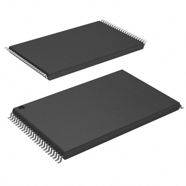
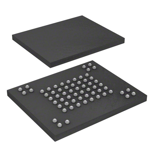
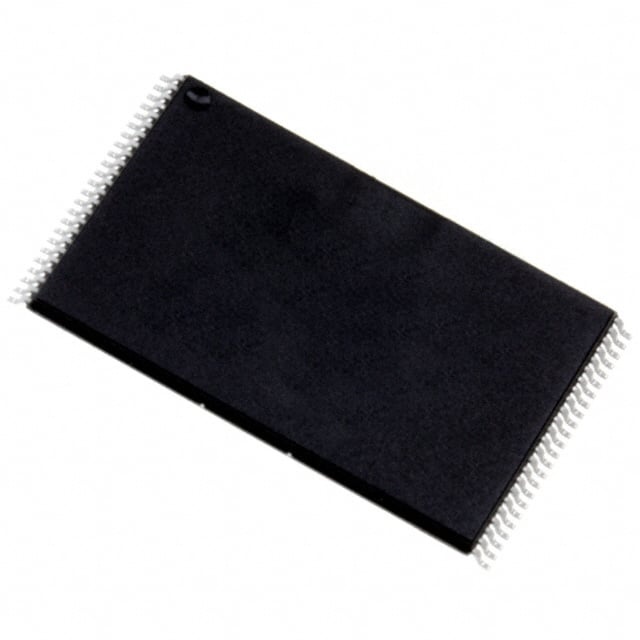
| Device Package | 63-VFBGA (9x11) | Memory Format | FLASH | Technology | FLASH - NAND | ||
|---|---|---|---|---|---|---|---|
| Memory Size | 512 Mbit | Access Time | 50 ns | Grade | Industrial | ||
| Clock Frequency | N/A | Voltage | 2.7V ~ 3.6V | Memory Type | Non-Volatile | ||
| Operating Temperature | -40°C ~ 85°C (TA) | Write Cycle Time Word Page | 50 ns | Packaging | 63-TFBGA | ||
| Mounting Method | Non-Volatile | Memory Interface | Parallel | Memory Organization | 64M x 8 | ||
| Moisture Sensitivity Level | 3 (168 Hours) | RoHS Compliance | ROHS3 Compliant | REACH Compliance | REACH Unaffected | ||
| Qualification | N/A | ECCN | 3A991B1A | HTS Code | 8542.32.0071 |
Overview of NAND512W3A2CZA6E – IC FLASH 512MBIT PAR 63VFBGA
The NAND512W3A2CZA6E is a 512‑Mbit parallel NAND flash memory device provided in a 63‑VFBGA (9×11) package. It implements SLC NAND architecture with a 64M × 8 organization and a 528‑byte / 264‑word page structure suitable for block‑oriented mass storage applications.
Designed for board‑level integration, the device operates from a 2.7 V to 3.6 V supply and across an ambient temperature range of −40 °C to 85 °C, offering programmable/erase endurance and built‑in management features for stored data integrity.
Key Features
- Memory Density & Organization 512‑Mbit capacity organized as 64M × 8 with a 528‑byte (x8) / 264‑word (x16) page format and dedicated spare bytes for management.
- NAND Interface & Bus Width Parallel NAND interface with support for x8 or x16 bus widths and multiplexed address/data signaling for standard NAND system integration.
- Performance Read/write timing suited for NAND applications: specified access time 50 ns and typical page program time of 200 μs; fast block erase typically 2 ms.
- Endurance & Data Integrity Designed with P/E endurance up to 100,000 cycles (with ECC) and 10‑year data retention; includes status register, electronic signature, OTP area, and hardware data protection features.
- Voltage & Temperature Operating supply voltage range 2.7 V to 3.6 V and operating ambient temperature from −40 °C to 85 °C for broad environmental compatibility.
- Package & Mounting Supplied in a 63‑VFBGA (9×11) package (63‑TFBGA notation) for compact PCB footprints and BGA mounting.
- Development & System Support Datasheet references development tools, ECC models, bad‑block management and wear‑leveling algorithms, and hardware simulation models to aid integration and validation.
- Design Status The datasheet notes the device is in production but not recommended for new designs.
Typical Applications
- Mass Storage Applications Cost‑effective NAND storage for mass storage use cases that require block‑oriented flash and spare‑area management.
- Managed NAND Systems Designs that implement ECC, bad‑block management and wear leveling can leverage the device’s spare area and available software models.
- Compact Board‑Level Storage BGA package (63‑VFBGA, 9×11) enables compact PCB layouts where board real estate is constrained.
Unique Advantages
- High density in a compact package: 512‑Mbit capacity in a 63‑VFBGA footprint minimizes board area for high‑capacity applications.
- Flexible interface options: Parallel NAND operation with x8/x16 bus widths supports integration into a variety of controller architectures.
- Designed for longevity: Up to 100,000 program/erase cycles (with ECC) and 10‑year data retention support long service life for stored data.
- System integration support: Provided development tools, ECC models and wear‑leveling guidance reduce integration effort and accelerate validation.
- Wide operating range: 2.7 V–3.6 V supply and −40 °C to 85 °C operating temperature cover many industrial and commercial environments.
- On‑device management features: Status register, electronic signature, OTP area and hardware data protection assist in system‑level data management and security.
Why Choose NAND512W3A2CZA6E?
The NAND512W3A2CZA6E provides a high‑capacity, parallel SLC NAND solution packaged for compact board designs, with timing, endurance and spare‑area features tailored to managed NAND storage applications. Its development resources—including ECC models and wear‑leveling algorithms—support engineers in implementing reliable NAND systems.
This device is suitable for designs requiring a 512‑Mbit parallel NAND flash with defined voltage and temperature ranges and a BGA package. Note that the datasheet specifies the product is still in production but not recommended for new designs.
Request a quote or submit an inquiry for pricing and availability to begin evaluating the NAND512W3A2CZA6E for your design needs.