
NAND512W3A2BZA6E
| Part Description |
IC FLASH 512MBIT PAR 63VFBGA |
|---|---|
| Quantity | 285 Available (as of June 10, 2026) |
| Product Category | Memory |
|---|---|
| Manufacturer | STMicroelectronics |
| Manufacturing Status | Obsolete |
| Manufacturer Standard Lead Time | Contact Us |
| Datasheet |
Specifications & Environmental
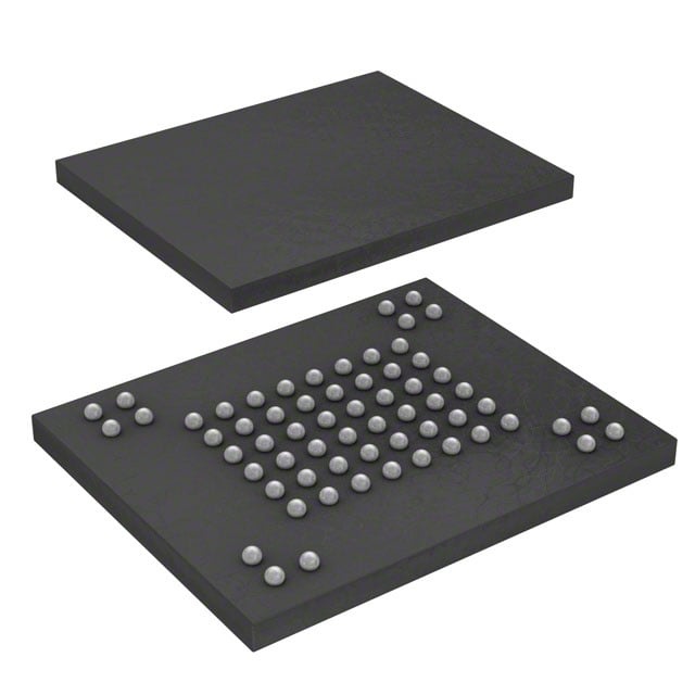
| Device Package | 63-VFBGA (8.5x15) | Memory Format | FLASH | Technology | FLASH - NAND | ||
|---|---|---|---|---|---|---|---|
| Memory Size | 512 Mbit | Access Time | 50 ns | Grade | Industrial | ||
| Clock Frequency | N/A | Voltage | 2.7V ~ 3.6V | Memory Type | Non-Volatile | ||
| Operating Temperature | -40°C ~ 85°C (TA) | Write Cycle Time Word Page | 50 ns | Packaging | 63-VFBGA | ||
| Mounting Method | Non-Volatile | Memory Interface | Parallel | Memory Organization | 64M x 8 | ||
| Moisture Sensitivity Level | 3 (168 Hours) | RoHS Compliance | ROHS3 Compliant | REACH Compliance | REACH Unaffected | ||
| Qualification | N/A | ECCN | 3A991B1A | HTS Code | 8542.32.0071 |
Overview of NAND512W3A2BZA6E – IC FLASH 512MBIT PAR 63VFBGA
The NAND512W3A2BZA6E is a 512 Mbit non-volatile NAND flash memory organized as 64M x 8, supplied in a 63-VFBGA package (8.5 × 15 mm). It implements a parallel NAND interface and is targeted for mass storage applications and embedded systems requiring dense, low-voltage flash memory.
Designed for system boot and data storage, the device offers fast sequential access and standard NAND features such as copy-back programming and automatic page 0 read at power-up to support system boot workflows.
Key Features
- Memory Core 512 Mbit NAND flash organized as 64M × 8 with x8 bus width; page size for x8 devices is 512 bytes plus 16 spare bytes.
- Interface Parallel NAND interface with multiplexed address/data pins and pinout compatibility across densities for straightforward board integration.
- Performance Sequential access down to 50 ns (min) and random page read typical/max values documented; page program time typical 200 µs and write-cycle timing supports 50 ns word/page cycles.
- Power 3.0 V device supply range: 2.7 V to 3.6 V for compatibility with common system rails.
- Package 63-VFBGA package, 8.5 × 15 mm footprint, suitable for compact board layouts.
- Reliability & Data Integrity Designed for 100,000 program/erase cycles and 10 years data retention; includes hardware data protection (program/erase locked during power transitions) and a status register for operation monitoring.
- System Features Copy-back program mode for fast internal page-to-page transfer, fast block erase (typical 2 ms), electronic signature, serial number option and automatic page 0 read at power-up for boot support.
- Development Support Datasheet notes availability of ECC models, bad block management and wear-leveling algorithms, demo hardware and reference software to assist integration and validation.
- Operating Range Specified operating ambient temperature range of −40 °C to 85 °C (TA) for a wide range of environments.
Typical Applications
- Mass storage devices Dense NAND array and spare-area architecture provide cost-effective storage for consumer and embedded mass-storage applications.
- Embedded system boot memory Automatic page 0 read at power-up option enables boot-from-NAND scenarios for embedded platforms.
- File-system and data logging 512 Mbit capacity with spare area supports file-system structures and wear management for data logging applications.
Unique Advantages
- High-density storage: 512 Mbit in a compact VFBGA package reduces board area while providing significant non-volatile capacity.
- Parallel NAND interface: x8 bus and multiplexed address/data reduce external buffering requirements and simplify host interface design.
- Boot support built-in: Automatic page 0 read at power-up facilitates system boot without additional boot ROM.
- Robust endurance and retention: 100,000 program/erase cycles and 10 years data retention support long-term field operation and data integrity.
- Design & validation resources: ECC models, wear-leveling and bad-block management algorithms, plus demo hardware and reference software streamline development and bring-up.
- Wide supply and temperature window: 2.7 V–3.6 V supply range and −40 °C to 85 °C operating range fit common system power rails and environmental requirements.
Why Choose IC FLASH 512MBIT PAR 63VFBGA?
The NAND512W3A2BZA6E positions itself as a high-density, parallel NAND flash option for designers needing compact, boot-capable non-volatile storage. Its combination of 512 Mbit capacity, fast sequential access, copy-back programming and power-up boot support addresses both mass-storage and embedded system requirements.
With documented endurance (100,000 P/E cycles), long data retention, and available development tools (ECC models, wear-leveling and demo hardware), this device is suitable for engineers seeking a verifiable solution for storage, boot memory and data-logging applications where footprint, integration and data integrity are priorities.
Request a quote or submit a product inquiry to receive pricing, availability and integration support for the NAND512W3A2BZA6E.


Date Founded: 1987
Headquarters: Plan-les-Ouates, Geneva, Switzerland
Employees: 50,000+
Revenue: $17.24 Billion
Certifications and Memberships: ISO9001:2015, ISO14001:2015, ISO45001:2018, IATF16949:2016, ISO50001:2018


