
NAND512W3A2BN6F
| Part Description |
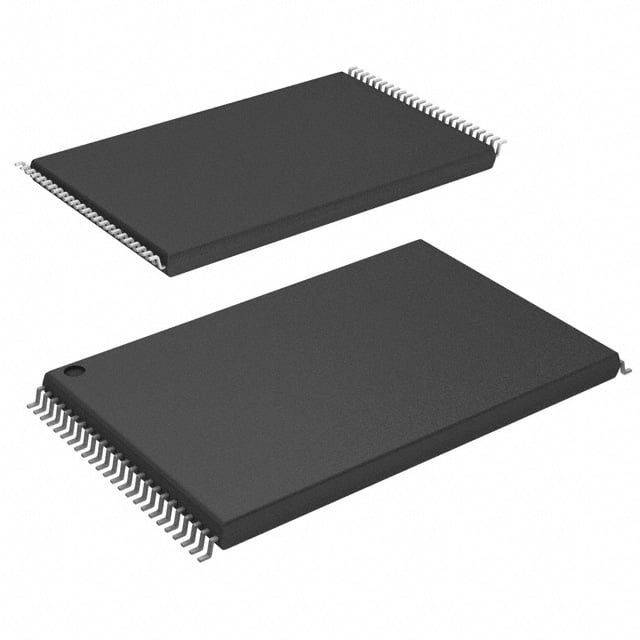
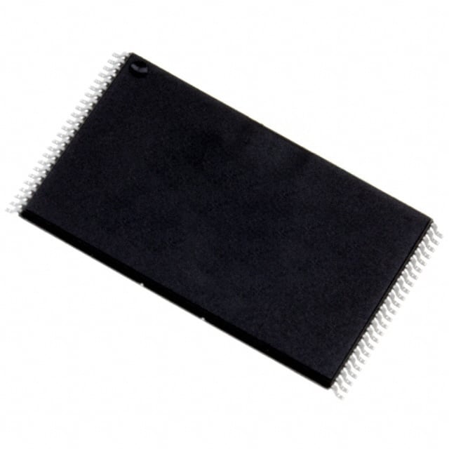
IC FLASH 512MBIT PARALLEL 48TSOP |
|---|---|
| Quantity | 621 Available (as of June 15, 2026) |

| Product Category | Memory |
|---|---|
| Manufacturer | STMicroelectronics |
| Manufacturing Status | Obsolete |
| Manufacturer Standard Lead Time | Contact Us |
| Datasheet |
Specifications & Environmental
| Device Package | 48-TSOP | Memory Format | FLASH | Technology | FLASH - NAND | ||
|---|---|---|---|---|---|---|---|
| Memory Size | 512 Mbit | Access Time | 50 ns | Grade | Industrial | ||
| Clock Frequency | N/A | Voltage | 2.7V ~ 3.6V | Memory Type | Non-Volatile | ||
| Operating Temperature | -40°C ~ 85°C (TA) | Write Cycle Time Word Page | 50 ns | Packaging | 48-TFSOP (0.724", 18.40mm Width) | ||
| Mounting Method | Non-Volatile | Memory Interface | Parallel | Memory Organization | 64M x 8 | ||
| Moisture Sensitivity Level | 3 (168 Hours) | RoHS Compliance | ROHS3 Compliant | REACH Compliance | REACH Unaffected | ||
| Qualification | N/A | ECCN | 3A991B1A | HTS Code | 8542.32.0071 |
Overview of NAND512W3A2BN6F – IC FLASH 512MBIT PARALLEL 48TSOP
The NAND512W3A2BN6F is a 512 Mbit non-volatile NAND Flash memory organized as 64M × 8 with a parallel NAND interface in a 48-TSOP (48-TFSOP) package. It targets high-density mass storage and embedded memory applications that require a compact TSOP form factor and standard NAND control signals.
Designed for 3.0 V systems (VDD = 2.7 V to 3.6 V) and industrial temperature ranges (–40 °C to 85 °C), the device provides page-level and block-level operations, hardware data protection during power transitions, and development support for error correction and bad-block management.
Key Features
- Memory Core 512 Mbit NAND Flash organized as 64M × 8 with x8 device page size of 512 + 16 spare bytes and block size of 16K + 512 spare bytes.
- Performance Random page access up to 12 µs (max) and sequential access down to 50 ns (min); typical page program time 200 µs and typical block erase time 2 ms.
- Interface & Signaling Parallel NAND interface with multiplexed address/data and pinout compatibility across densities; supports chip enable “don’t care” option for simplified interfacing with microcontrollers.
- Power Single-supply operation for the 3.0 V family: VDD = 2.7 V to 3.6 V.
- Reliability & Data Integrity Hardware data protection (program/erase locked during power transitions), endurance of 100,000 program/erase cycles and data retention of 10 years.
- Boot & Utility Features Automatic page 0 read at power-up option for boot-from-NAND support and fast copy-back program mode for internal page-to-page transfers without external buffering.
- Package & Temperature Supplied in a 48-TFSOP/TSOP package (0.724", 18.40 mm width) and specified for operation from –40 °C to 85 °C.
- Development Tools Error correction code software and hardware models, bad-block management and wear-leveling algorithm references, and PC demo board support are provided for integration and validation.
Typical Applications
- Mass storage devices — Cost-effective NAND Flash capacity for applications requiring high-density non-volatile storage.
- Embedded boot and firmware storage — Automatic page 0 read at power-up enables boot-from-NAND scenarios and automatic memory download.
- Microcontroller-based systems — Parallel NAND interface and chip-enable flexibility simplify integration with microcontroller hosts for code and data storage.
- General embedded memory — Page and block operation timings, plus endurance and retention specs, support long-lived embedded storage functions.
Unique Advantages
- High-density NAND in a compact TSOP — 512 Mbit capacity in a 48-TSOP package reduces PCB area for high-capacity embedded designs.
- Fast sequential access — Sequential access down to 50 ns supports efficient data throughput for page-level operations.
- Robust endurance and retention — 100,000 program/erase cycles and 10 years retention give predictable life characteristics for deployed systems.
- Power-up boot support — Automatic page 0 read simplifies system boot architecture and reduces external boot ROM requirements.
- Integration and design support — Provided ECC models, bad-block management and wear-leveling algorithms accelerate development and validation.
- Wide supply range — 2.7 V to 3.6 V operation provides compatibility with typical 3.0 V embedded power architectures.
Why Choose NAND512W3A2BN6F?
NAND512W3A2BN6F delivers a high-density, industrial-temperature NAND Flash option packaged in a standard 48-TSOP footprint. Its combination of 512 Mbit capacity, parallel x8 interface, and device-level features such as automatic page 0 read and copy-back program mode make it suitable for designs that require compact mass storage, firmware boot capability, and predictable endurance.
Backed by STMicroelectronics’ development resources — including ECC and bad-block management models and demo hardware — this device is positioned for engineering teams building embedded storage and boot systems that need verifiable specifications for performance, reliability, and integration.
Request a quote or submit a pricing inquiry to evaluate NAND512W3A2BN6F for your next design.


Date Founded: 1987
Headquarters: Plan-les-Ouates, Geneva, Switzerland
Employees: 50,000+
Revenue: $17.24 Billion
Certifications and Memberships: ISO9001:2015, ISO14001:2015, ISO45001:2018, IATF16949:2016, ISO50001:2018


