W9412G6JH-5I
| Part Description |
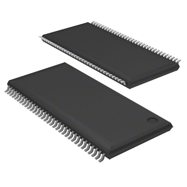
IC DRAM 128MBIT SSTL2 66TSOP II |
|---|---|
| Quantity | 1,889 Available (as of June 15, 2026) |

| Product Category | DRAM Memory |
|---|---|
| Manufacturer | Winbond Electronics |
| Manufacturing Status | Obsolete |
| Manufacturer Standard Lead Time | Contact Us |
| Datasheet |
Specifications & Environmental
| Device Package | 66-TSOP II | Memory Format | DRAM | Technology | SDRAM - DDR | ||
|---|---|---|---|---|---|---|---|
| Memory Size | 128 Mbit | Access Time | 50 ns | Grade | Industrial | ||
| Clock Frequency | 200 MHz | Voltage | 2.3V ~ 2.7V | Memory Type | Volatile | ||
| Operating Temperature | -40°C ~ 85°C (TA) | Write Cycle Time Word Page | 15 ns | Packaging | 66-TSSOP (0.400", 10.16mm Width) | ||
| Mounting Method | Volatile | Memory Interface | SSTL_2 | Memory Organization | 8M x 16 | ||
| Moisture Sensitivity Level | 3 (168 Hours) | RoHS Compliance | ROHS3 Compliant | REACH Compliance | REACH Unaffected | ||
| Qualification | N/A | ECCN | EAR99 | HTS Code | 8542.32.0002 |
Overview of W9412G6JH-5I – IC DRAM 128MBIT SSTL2 66TSOP II
The W9412G6JH-5I is a 128 Mbit DDR SDRAM device in a 66-TSSOP (66-TSOP II) package. It implements a multi-bank DDR architecture with an SSTL_2 memory interface and is optimized for board-level memory applications requiring a compact footprint.
Key attributes include a 200 MHz clock rating for DDR operation, a 2.3 V–2.7 V supply range, and an operating temperature window from −40°C to 85°C, providing deterministic electrical and timing characteristics for system designers.
Key Features
- Memory Core 128 Mbit DDR SDRAM organized as 8M × 16, with multi-bank DDR architecture (documented as 2M × 4 banks × 16 bits in the datasheet).
- Performance Supports DDR operation with a clock frequency up to 200 MHz and an access time of 50 ns; write cycle time (word page) specified at 15 ns.
- Interface SSTL_2 memory interface for systems using SSTL_2 signaling conventions.
- Command and Mode Support Implements the standard DDR command set including bank activate, precharge, auto-refresh, self-refresh, mode register set and extended mode register operations as detailed in the datasheet.
- Power Recommended supply voltage range of 2.3 V to 2.7 V with defined power-up sequencing and power-down/self-refresh modes described in the datasheet.
- Package & Temperature Available in a 66-TSSOP (0.400", 10.16 mm width) TSOP II package; operating temperature range −40°C to 85°C for deployment across commercial and industrial ambient conditions.
- Electrical and Timing Documentation Comprehensive electrical characteristics, AC timing, and system-level timing guidance (input/output setup & hold, slew rate, timing waveforms) are provided in the product datasheet.
Typical Applications
- Systems requiring SSTL_2 memory interfaces Use the W9412G6JH-5I where an SSTL_2 DDR memory interface and 128 Mbit density are required on the board.
- Compact board-level memory The 66-TSSOP II package suits designs with limited PCB area that need DDR SDRAM density in a narrow footprint.
- Temperature-sensitive deployments Applications that require operation across −40°C to 85°C can leverage the specified operating range.
Unique Advantages
- Compact TSOP II footprint: Enables space-efficient board layouts with a 66-TSSOP (0.400", 10.16 mm width) package.
- SSTL_2 compatibility: Direct fit for systems using SSTL_2 signaling, simplifying interface design.
- Documented DDR command support: Full command set and mode register functionality are specified, aiding predictable memory control and sequencing.
- Wide operating voltage window: 2.3 V to 2.7 V supply range accommodates common DDR supply rails.
- Industrial temperature range: Rated for −40°C to 85°C operation to support broader ambient conditions.
- Comprehensive timing and electrical data: Datasheet includes AC characteristics, timing waveforms, and system-level guidance for signal integrity and timing margins.
Why Choose IC DRAM 128MBIT SSTL2 66TSOP II?
The W9412G6JH-5I provides a focused DDR SDRAM solution for designs that need 128 Mbit density in a narrow 66-TSSOP II package with SSTL_2 signaling. Its documented timing, command set, and electrical characteristics allow engineers to integrate the device with predictable behavior at up to 200 MHz DDR clock rates.
This device is suited for board-level memory implementations that prioritize a compact footprint, defined operating voltage (2.3 V–2.7 V), and a broad operating temperature range (−40°C to 85°C). The detailed datasheet content supports system validation, timing closure, and reliable memory operation within the specified parameters.
Request a quote or submit a pricing and availability inquiry to receive product information and lead-time details for the W9412G6JH-5I.