W9725G6JB25I
| Part Description |
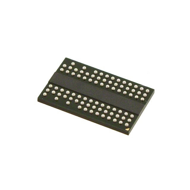
IC DRAM 256MBIT PAR 84WBGA |
|---|---|
| Quantity | 121 Available (as of June 15, 2026) |

| Product Category | Memory |
|---|---|
| Manufacturer | Winbond Electronics |
| Manufacturing Status | Obsolete |
| Manufacturer Standard Lead Time | Contact Us |
| Datasheet |
Specifications & Environmental
| Device Package | 84-WBGA (8x12.5) | Memory Format | DRAM | Technology | SDRAM - DDR2 | ||
|---|---|---|---|---|---|---|---|
| Memory Size | 256 Mbit | Access Time | 52.5 ns | Grade | Automotive | ||
| Clock Frequency | 200 MHz | Voltage | 1.7V ~ 1.9V | Memory Type | Volatile | ||
| Operating Temperature | -40°C ~ 95°C (TC) | Write Cycle Time Word Page | 15 ns | Packaging | 84-TFBGA | ||
| Mounting Method | Volatile | Memory Interface | Parallel | Memory Organization | 16M x 16 | ||
| Moisture Sensitivity Level | 3 (168 Hours) | RoHS Compliance | ROHS3 Compliant | REACH Compliance | REACH Unaffected | ||
| Qualification | N/A | ECCN | EAR99 | HTS Code | 8542.32.0036 |
Overview of W9725G6JB25I – 256 Mbit DDR2 SDRAM (84-WBGA)
The W9725G6JB25I is a 256 Mbit volatile DDR2 SDRAM device organized as 16M × 16 (4M × 4 banks × 16‑bit). It implements a parallel DDR2 memory interface and supports core DDR2 control features and modes as documented in the device datasheet.
Designed for applications requiring a compact 84‑ball WBGA package and operation over a broad temperature range, the device offers timing, mode and termination controls suitable for embedded and system memory subsystems operating with a 1.7–1.9 V supply.
Key Features
- Memory Core 256 Mbit DDR2 SDRAM organized as 16M × 16 (4M × 4 banks × 16‑bit) for parallel DRAM implementations.
- Performance Supports a 200 MHz clock frequency with an access time of 52.5 ns and a write cycle time (word page) of 15 ns.
- Voltage and Power Operates from a 1.7 V to 1.9 V supply; includes power-down and self-refresh operation modes described in the datasheet.
- Control and Register Features Mode Register Set (MRS) and Extended Mode Register (EMRS) operations are supported, including DLL enable/disable, Off‑Chip Driver (OCD) impedance adjustment and On‑Die Termination (ODT) control.
- Burst and Command Support Supports burst read/write operations, posted CAS behavior, auto‑precharge commands and standard DDR2 command sequences for flexible data transfer patterns.
- Package and Temperature Available in an 84‑TFBGA / 84‑WBGA (8 × 12.5 mm) supplier package with an operating temperature range of -40°C to 95°C (TC).
- Interface Parallel memory interface in DRAM format with 16‑bit data organization suitable for systems requiring parallel DDR2 memory.
Typical Applications
- Embedded memory subsystems — Provides 256 Mbit DDR2 storage in designs that require a parallel DDR2 interface and 16‑bit data organization.
- Industrial systems — Operating temperature range of -40°C to 95°C supports deployment in temperature‑sensitive industrial environments.
- Board‑level buffering — Parallel interface and burst support enable use as a buffer or temporary frame/storage memory in systems that use DDR2 signaling.
Unique Advantages
- Compact WBGA footprint: 84‑ball WBGA (8 × 12.5 mm) package option minimizes board area for dense system layouts.
- Broad operating temperature: -40°C to 95°C rating supports a wide range of environmental conditions.
- Flexible timing control: Mode register and extended mode register support, DLL control and ODT/OCD features allow fine tuning of timing and termination.
- Measured performance metrics: 200 MHz clock, 52.5 ns access time and 15 ns word‑page write cycle time give clear, verifiable timing characteristics for system integration.
- Low‑voltage DDR2 operation: 1.7 V–1.9 V supply aligns with DDR2 power domains for compatible system designs.
Why Choose W9725G6JB25I?
The W9725G6JB25I positions itself as a 256 Mbit DDR2 parallel DRAM option that combines a 16M × 16 organization and standard DDR2 control features with a compact 84‑WBGA package. Its documented command, register and termination controls (including MRS/EMRS, DLL, ODT and OCD) provide the configuration flexibility needed for precise timing and signal integrity tuning.
This device is suited to designers who need verifiable DDR2 timing (200 MHz clock, specific access and cycle times), operation across an extended temperature range, and a small BGA footprint. The included datasheet content details operational modes, electrical characteristics and timing parameters to support engineering integration and validation.
Request a quote or contact our sales team to discuss availability, lead times and pricing for the W9725G6JB25I.