W9751G6KB-25 TR
| Part Description |
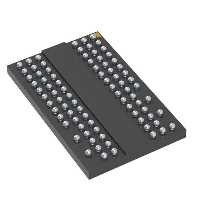
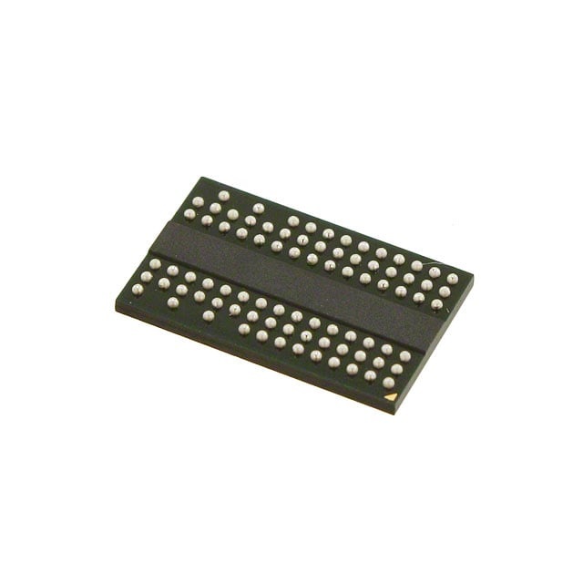
IC DRAM 512MBIT PARALLEL 84WBGA |
|---|---|
| Quantity | 1,440 Available (as of June 15, 2026) |
| Product Category | Memory |
|---|---|
| Manufacturer | Winbond Electronics |
| Manufacturing Status | Obsolete |
| Manufacturer Standard Lead Time | Contact Us |
| Datasheet |
Specifications & Environmental
| Device Package | 84-WBGA (8x12.5) | Memory Format | DRAM | Technology | SDRAM - DDR2 | ||
|---|---|---|---|---|---|---|---|
| Memory Size | 512 Mbit | Access Time | 57.5 ns | Grade | Commercial (Extended) | ||
| Clock Frequency | 400 MHz | Voltage | 1.7V ~ 1.9V | Memory Type | Volatile | ||
| Operating Temperature | 0°C ~ 85°C (TC) | Write Cycle Time Word Page | 15 ns | Packaging | 84-TFBGA | ||
| Mounting Method | Volatile | Memory Interface | Parallel | Memory Organization | 32M x 16 | ||
| Moisture Sensitivity Level | 3 (168 Hours) | RoHS Compliance | ROHS3 Compliant | REACH Compliance | REACH Unaffected | ||
| Qualification | N/A | ECCN | EAR99 | HTS Code | 8542.32.0028 |
Overview of W9751G6KB-25 TR – IC DRAM 512MBIT PARALLEL 84WBGA
The W9751G6KB-25 TR is a 512 Mbit DDR2 SDRAM device organized as 32M × 16 with an 8M × 4 banks × 16 bit architecture. It provides a parallel memory interface in an 84-WBGA (8 × 12.5 mm) package and is specified for 1.7 V to 1.9 V supply operation and an operating temperature range of 0°C to 85°C.
Designed for applications that require standard DDR2 synchronous DRAM behavior, the device documentation includes detailed support for mode register programming, on-die termination (ODT), DLL control, extended mode registers (EMR), refresh, power-down and self-refresh sequences, and impedance adjustment routines to assist system memory integration.
Key Features
- Memory Core — 512 Mbit DDR2 SDRAM organized as 32M × 16 (8M × 4 banks × 16 bit) to provide parallel DDR2 memory architecture and banked operation.
- Performance — Operates with a clock frequency up to 400 MHz and specified access time of 57.5 ns; supports DDR2 burst and posted CAS/burst modes as described in the device functional documentation.
- Voltage and Timing — Specified supply voltage range of 1.7 V to 1.9 V and a write cycle time (word page) of 15 ns, with comprehensive AC timing and command operation tables in the datasheet.
- On-Chip Control and Configuration — Datasheet details include Mode Register Set (MRS), Extended Mode Registers (EMR), DLL enable/disable, On-Die Termination (ODT), and Off-Chip Driver (OCD) impedance adjustment for runtime configuration and signal integrity tuning.
- Power Management — Functional descriptions cover power-up/initialization, refresh, power-down, and self-refresh modes to support controlled low-power and retention behaviors.
- Package — 84-TFBGA / 84-WBGA (8 × 12.5 mm) package case suitable for surface-mount assembly with ball configuration and pin descriptions provided in the documentation.
- Operating Range — Specified operating temperature condition of 0°C to 85°C as provided in the product specifications and datasheet.
Typical Applications
- Embedded memory subsystems — Use as a 512 Mbit parallel DDR2 memory device in embedded designs requiring banked DDR2 SDRAM and documented mode register control.
- Board-level DRAM modules — Integration into custom memory modules or carrier boards where an 84-WBGA footprint and 1.7 V–1.9 V DDR2 operation are required.
- System memory for synchronous designs — Implement as parallel DDR2 SDRAM for systems that leverage burst read/write and posted CAS features documented in the device specification.
Unique Advantages
- Banked DDR2 architecture: 8M × 4 banks × 16 bit organization enables standard DDR2 banked operations as documented for efficient burst access patterns.
- Configurable termination and drivers: Includes documented ODT and OCD impedance adjustment and extended mode registers for tuning signal integrity on populated systems.
- Compact WBGA package: 84-ball WBGA (8 × 12.5 mm) package minimizes PCB footprint while providing a defined ball configuration and placement information in the datasheet.
- Comprehensive control sequencing: Datasheet provides detailed power-up/initialization, refresh, power-down and self-refresh sequences that support predictable memory behavior in system designs.
- Tight supply and timing specification: Operation at 1.7 V–1.9 V with specified clock frequency and timing parameters aids deterministic design and validation against the provided AC/DC characteristics.
Why Choose W9751G6KB-25 TR?
The W9751G6KB-25 TR is positioned as a standardized DDR2 SDRAM component offering a 512 Mbit density in a 32M × 16 organization with documented mode, timing, and termination controls. Its datasheet includes detailed electrical and timing characteristics, command sequences, and configuration options (MRS/EMR, ODT, DLL, OCD) to support integration into synchronous memory subsystems.
This device is appropriate for designers and procurement teams specifying a parallel DDR2 memory device with defined supply range (1.7 V–1.9 V), 0°C–85°C operating temperature, and a compact 84-WBGA package where detailed configuration and signal integrity controls are required for board-level integration.
If you require pricing or availability details or want to request a formal quote for W9751G6KB-25 TR, please submit a request for a quote or contact our sales channel to discuss your project requirements.