W9751G6KB25I
| Part Description |
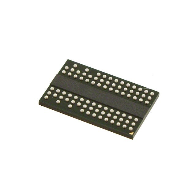
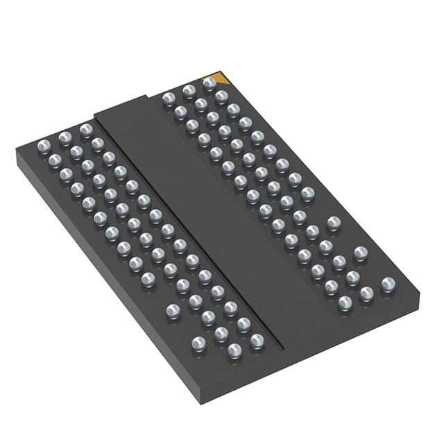
IC DRAM 512MBIT PARALLEL 84WBGA |
|---|---|
| Quantity | 475 Available (as of June 15, 2026) |

| Product Category | Memory |
|---|---|
| Manufacturer | Winbond Electronics |
| Manufacturing Status | Obsolete |
| Manufacturer Standard Lead Time | Contact Us |
| Datasheet |
Specifications & Environmental
| Device Package | 84-WBGA (8x12.5) | Memory Format | DRAM | Technology | SDRAM - DDR2 | ||
|---|---|---|---|---|---|---|---|
| Memory Size | 512 Mbit | Access Time | 57.5 ns | Grade | Automotive | ||
| Clock Frequency | 400 MHz | Voltage | 1.7V ~ 1.9V | Memory Type | Volatile | ||
| Operating Temperature | -40°C ~ 95°C (TC) | Write Cycle Time Word Page | 15 ns | Packaging | 84-TFBGA | ||
| Mounting Method | Volatile | Memory Interface | Parallel | Memory Organization | 32M x 16 | ||
| Moisture Sensitivity Level | 3 (168 Hours) | RoHS Compliance | ROHS3 Compliant | REACH Compliance | REACH Unaffected | ||
| Qualification | N/A | ECCN | EAR99 | HTS Code | 8542.32.0024 |
Overview of W9751G6KB25I – DDR2 SDRAM 512 Mbit, 84‑WBGA
The W9751G6KB25I is a 512 Mbit DDR2 SDRAM device organized as 32M × 16 with a parallel memory interface. It implements a multi‑bank DDR2 architecture (8M × 4 banks × 16‑bit as referenced in the datasheet) and operates from a 1.7 V to 1.9 V supply.
Key electrical and timing characteristics include a 400 MHz clock frequency, 57.5 ns access time, and a word/page write cycle time of 15 ns. The device is supplied in an 84‑ball WBGA package with an operating temperature range of −40 °C to 95 °C (TC).
Key Features
- Memory Architecture DDR2 SDRAM organized as 32M × 16 (512 Mbit) with internal bank structure described as 8M × 4 banks × 16‑bit in the datasheet.
- Performance Supports a 400 MHz clock frequency with a specified access time of 57.5 ns and a write cycle time (word/page) of 15 ns for predictable timing behavior.
- Power Operates from a 1.7 V to 1.9 V supply voltage range and includes power management modes referenced in the datasheet such as power‑down and self‑refresh.
- Signal Integrity and Control On‑die termination (ODT), off‑chip driver (OCD) impedance adjustment, DLL enable/disable and multiple mode/extended mode register controls are documented in the device specification for drive and timing configuration.
- Command and Functional Support Supports standard DDR2 command set and operations described in the datasheet, including bank activate, read, write, burst read/write, auto‑precharge, refresh, power‑down, and self‑refresh sequences.
- Packaging and Temperature Offered in an 84‑TFBGA / 84‑WBGA (8 × 12.5 mm) package with an operating temperature range of −40 °C to 95 °C (TC) suitable for extended temperature deployments.
Typical Applications
- Parallel DDR2 memory subsystems — 512 Mbit density and a parallel DDR2 interface for designs that require synchronous burst access and banked memory organization.
- Board‑level DRAM modules — 84‑WBGA package and compact footprint for integration into board‑level memory solutions.
- Thermally demanding environments — Rated −40 °C to 95 °C (TC) for use where extended temperature range operation is required.
Unique Advantages
- 512 Mbit density in a compact package — 32M × 16 organization delivers substantial storage capacity within an 84‑ball WBGA footprint.
- DDR2 timing and banked architecture — Multi‑bank DDR2 structure (8M × 4 banks × 16‑bit) with documented burst and precharge operations supports standard DDR2 access patterns.
- Integrated drive and termination features — On‑die termination (ODT) and OCD impedance adjustment options are available as documented, enabling on‑chip signal termination control.
- Extended temperature rating — −40 °C to 95 °C (TC) operating range supports deployments across a wide ambient temperature span.
- Low‑voltage DDR2 supply — 1.7 V to 1.9 V supply range aligns with DDR2 power domains and system power budgeting requirements.
Why Choose W9751G6KB25I?
The W9751G6KB25I provides a straightforward DDR2 SDRAM option when a 512 Mbit parallel memory solution is required. Its documented DDR2 features—including multi‑bank organization, mode/extended mode register controls, ODT and OCD options, and standard DDR2 command support—offer designers clear configuration and timing references for system integration.
This device is suited to designs that require 32M × 16 organization, supported timing parameters (400 MHz clock frequency, 57.5 ns access time, 15 ns write cycle time), and a compact 84‑WBGA package with an extended operating temperature range, offering a verifiable, specification‑driven memory choice for compatible DDR2 system implementations.
Please request a quote or submit a product inquiry for the W9751G6KB25I to begin procurement or to obtain volume and lead‑time information.