W9751G6NB-25
| Part Description |
IC DRAM 512MBIT PAR 84VFBGA |
|---|---|
| Quantity | 971 Available (as of June 15, 2026) |

| Product Category | Memory |
|---|---|
| Manufacturer | Winbond Electronics |
| Manufacturing Status | Active |
| Manufacturer Standard Lead Time | 24 Weeks |
| Datasheet |
Specifications & Environmental
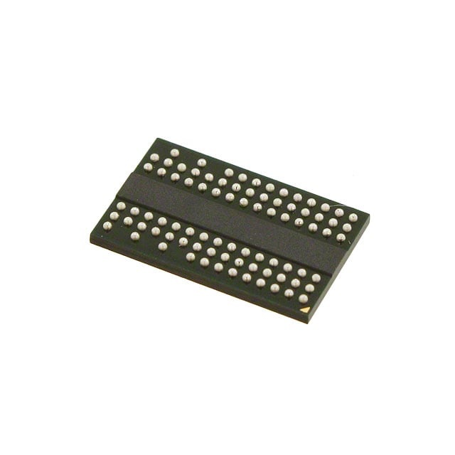
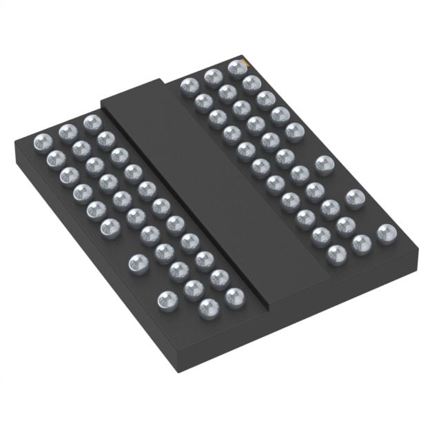
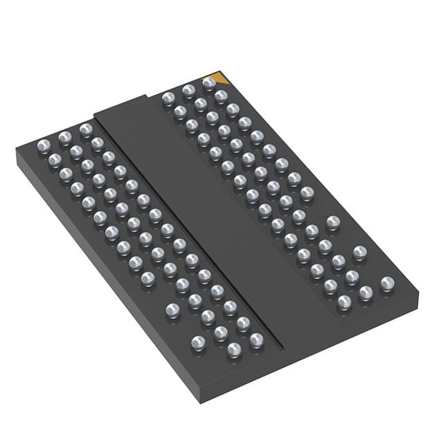
| Device Package | 84-VFBGA (8x12.5) | Memory Format | DRAM | Technology | SDRAM - DDR2 | ||
|---|---|---|---|---|---|---|---|
| Memory Size | 512 Mbit | Access Time | 57.5 ns | Grade | Commercial (Extended) | ||
| Clock Frequency | 400 MHz | Voltage | 1.7V ~ 1.9V | Memory Type | Volatile | ||
| Operating Temperature | 0°C ~ 85°C (TC) | Write Cycle Time Word Page | 15 ns | Packaging | 84-VFBGA | ||
| Mounting Method | Volatile | Memory Interface | Parallel | Memory Organization | 32M x 16 | ||
| Moisture Sensitivity Level | 3 (168 Hours) | RoHS Compliance | ROHS3 Compliant | REACH Compliance | REACH Unaffected | ||
| Qualification | N/A | ECCN | EAR99 | HTS Code | 8542.32.0028 |
Overview of W9751G6NB-25 – IC DRAM 512MBIT PAR 84VFBGA
The W9751G6NB-25 is a 512 Mbit DDR2 SDRAM organized as 32M × 16 with an 8M × 4 banks × 16-bit architecture. It provides a parallel DDR2 memory interface in an 84-VFBGA package for designs that require synchronous DRAM with on-die features exposed in the device documentation.
Key electrical and timing characteristics include a 400 MHz clock frequency, 1.7 V–1.9 V supply range, 57.5 ns access time, and an operating temperature range of 0°C to 85°C. The device datasheet documents mode register control, on-die termination (ODT), DLL enable/disable, and refresh/power-management sequences.
Key Features
- DDR2 SDRAM Core Synchronous DDR2 architecture with detailed mode register and extended mode register operations described in the datasheet (including MRS and EMRS commands).
- Memory Organization 32M × 16 organization presented as 8M × 4 banks × 16 bits, yielding a total density of 512 Mbit.
- High‑speed Operation Supports a clock frequency of 400 MHz and documented AC timing parameters for the -25 speed grade.
- Timing and Access Specified access time of 57.5 ns and write cycle time (word page) of 15 ns with full command set timing and waveforms provided.
- Low‑Voltage Supply Nominal supply range from 1.7 V to 1.9 V for DDR2 operation.
- On‑die Control Features Datasheet includes on-die termination (ODT), off-chip driver (OCD) impedance adjustment, DLL enable/disable, and related timing requirements.
- Package 84‑VFBGA package (8 × 12.5 mm) for compact mounting and board-level integration.
- Operating Conditions Specified commercial temperature range of 0°C to 85°C and full electrical/AC characteristic tables in the documentation.
Unique Advantages
- Deterministic DDR2 interface: The parallel DDR2 architecture and comprehensive command/timing definitions enable predictable memory timing integration for synchronous systems.
- Compact BGA footprint: The 84‑VFBGA (8 × 12.5 mm) package offers a space-efficient mounting option for board-level designs requiring DRAM density.
- Low-voltage operation: 1.7 V–1.9 V supply range reduces bus power compared with higher-voltage memory options while matching DDR2 power domains.
- On-die termination and impedance control: ODT and OCD impedance adjustment options documented in the datasheet help optimize signal integrity and PCB design margins.
- Comprehensive documentation: Detailed datasheet content covers mode register programming, refresh and power‑down sequences, and AC/DC characteristics to support integration and validation.
- Full timing visibility: AC characteristics, timing waveforms, and command function descriptions are provided to support accurate timing closure and system-level validation.
Why Choose W9751G6NB-25?
The W9751G6NB-25 positions itself as a standard DDR2 parallel DRAM device offering 512 Mbit density, documented timing for the -25 speed grade, and on-die features such as ODT and DLL control. Its combination of 400 MHz clock support, 1.7 V–1.9 V operation, and an 84‑VFBGA package make it well suited for designs that require a compact, documented DDR2 memory component with explicit command, timing, and electrical behavior available in the datasheet.
Design teams integrating the W9751G6NB-25 gain access to detailed operational sequences (power-up/initialization, mode register programming, refresh, and power‑down), AC/DC characteristic tables, and timing waveforms to aid system validation and board-level implementation.
If you need pricing, availability, or a formal quote for W9751G6NB-25, request a quote or contact sales to discuss availability and ordering details.