W9751G6NB-25 TR
| Part Description |
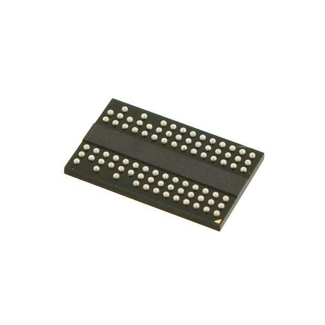
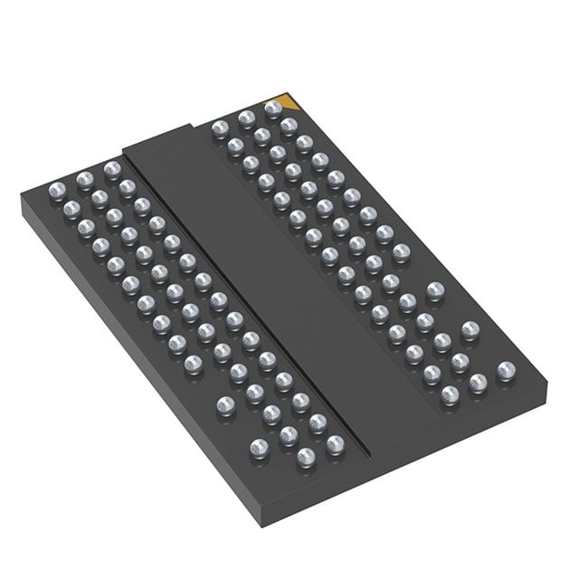
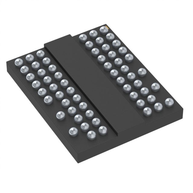
IC DRAM 512MBIT PAR 84VFBGA |
|---|---|
| Quantity | 890 Available (as of June 15, 2026) |

| Product Category | DRAM Memory |
|---|---|
| Manufacturer | Winbond Electronics |
| Manufacturing Status | Active |
| Manufacturer Standard Lead Time | 24 Weeks |
| Datasheet |
Specifications & Environmental
| Device Package | 84-VFBGA (8x12.5) | Memory Format | DRAM | Technology | SDRAM - DDR2 | ||
|---|---|---|---|---|---|---|---|
| Memory Size | 512 Mbit | Access Time | 57.5 ns | Grade | Commercial (Extended) | ||
| Clock Frequency | 400 MHz | Voltage | 1.7V ~ 1.9V | Memory Type | Volatile | ||
| Operating Temperature | 0°C ~ 85°C (TC) | Write Cycle Time Word Page | 15 ns | Packaging | 84-VFBGA | ||
| Mounting Method | Volatile | Memory Interface | Parallel | Memory Organization | 32M x 16 | ||
| Moisture Sensitivity Level | 3 (168 Hours) | RoHS Compliance | ROHS3 Compliant | REACH Compliance | REACH Unaffected | ||
| Qualification | N/A | ECCN | EAR99 | HTS Code | 8542.32.0028 |
Overview of W9751G6NB-25 TR – IC DRAM 512MBIT PAR 84VFBGA
The W9751G6NB-25 TR from Winbond Electronics is a 512 Mbit DDR2 SDRAM device organized as 32M × 16 (8M × 4 banks × 16 bit). It implements a parallel DDR2 memory interface in a compact 84‑VFBGA package.
Designed for systems requiring synchronous DDR2 DRAM with configurable mode registers and on‑die termination control, the device provides 400 MHz clock operation, a 1.7 V–1.9 V supply window, and an operating temperature range of 0°C to 85°C (TC).
Key Features
- Memory capacity and organization — 512 Mbit DRAM organized as 32M × 16 with 8M × 4 banks × 16‑bit architecture for standard DDR2 banked operation.
- DDR2 performance — Rated for a 400 MHz clock frequency with an access time of 57.5 ns and a write cycle time (word/page) of 15 ns.
- Parallel memory interface — Standard parallel DDR2 interface for synchronous read/write access and burst operations.
- Power supply — Operates from a 1.7 V to 1.9 V supply range consistent with DDR2 signaling.
- Functional controls — Supports Mode Register Set (MRS), Extended Mode Registers (EMRS), DLL enable/disable, On‑Die Termination (ODT) and related configuration features as described in the device documentation.
- Package and mounting — 84‑ball VFBGA package (8 × 12.5 mm) for compact surface‑mount applications.
- Environmental range — Specified operating temperature range of 0°C to 85°C (TC).
Unique Advantages
- Compact footprint: The 84‑VFBGA (8×12.5 mm) package minimizes board area while providing full DDR2 functionality for space‑constrained designs.
- High clock capability: 400 MHz rated clock frequency supports higher DDR2 throughput where synchronous memory performance is required.
- Configurable memory behavior: On‑die termination, DLL control and extended mode registers enable system‑level tuning of timing and drive characteristics.
- Standard DDR2 supply compatibility: 1.7 V–1.9 V operating range aligns with DDR2 power rails for straightforward system integration.
- Banked architecture: 8M × 4 bank organization supports typical DDR2 burst and page operations for efficient memory access patterns.
Why Choose IC DRAM 512MBIT PAR 84VFBGA?
The W9751G6NB-25 TR offers a compact, banked DDR2 SDRAM solution with explicit configuration controls (MRS/EMRS/ODT/DLL) and a 400 MHz clock rating, making it suitable for designs requiring synchronous parallel DRAM in a small VFBGA footprint. Its 1.7 V–1.9 V supply range and documented timing parameters support integration into DDR2 memory subsystems where controlled timing and termination are needed.
This device is appropriate for engineering teams and procurement looking for a documented DDR2 memory component with clear electrical and timing specifications and package details for PCB layout and system validation.
Request a quote or submit a parts inquiry to receive pricing and lead‑time information for the W9751G6NB-25 TR.