W9751G8NB25I
| Part Description |
IC DRAM 512MBIT PAR 60VFBGA |
|---|---|
| Quantity | 47 Available (as of June 15, 2026) |
| Product Category | Memory |
|---|---|
| Manufacturer | Winbond Electronics |
| Manufacturing Status | Active |
| Manufacturer Standard Lead Time | 24 Weeks |
| Datasheet |
Specifications & Environmental
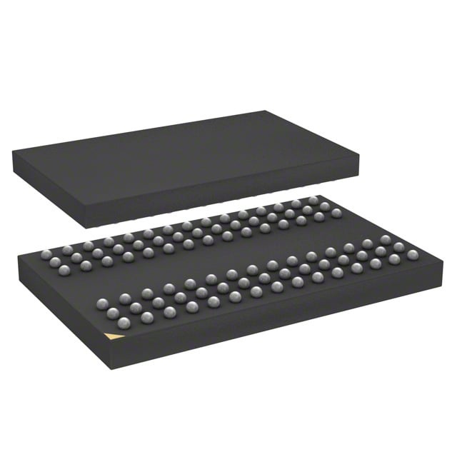
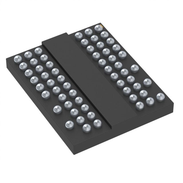
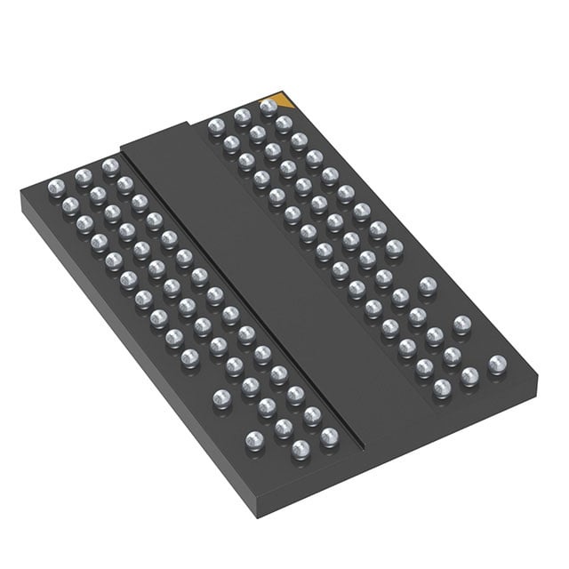
| Device Package | 60-VFBGA (8x9.5) | Memory Format | DRAM | Technology | SDRAM - DDR2 | ||
|---|---|---|---|---|---|---|---|
| Memory Size | 512 Mbit | Access Time | 57.5 ns | Grade | Automotive | ||
| Clock Frequency | 400 MHz | Voltage | 1.7V ~ 1.9V | Memory Type | Volatile | ||
| Operating Temperature | -40°C ~ 95°C (TC) | Write Cycle Time Word Page | 15 ns | Packaging | 60-VFBGA | ||
| Mounting Method | Volatile | Memory Interface | Parallel | Memory Organization | 64M x 8 | ||
| Moisture Sensitivity Level | 3 (168 Hours) | RoHS Compliance | ROHS Compliant | REACH Compliance | REACH Unaffected | ||
| Qualification | N/A | ECCN | EAR99 | HTS Code | 8542.32.0028 |
Overview of W9751G8NB25I – 512 Mbit DDR2 SDRAM, 60‑VFBGA
The W9751G8NB25I is a 512 Mbit parallel DDR2 SDRAM device organized as 64M × 8 and described in the datasheet as a 16M × 4 banks × 8‑bit DDR2 SDRAM. It implements standard DDR2 command and configuration functionality, including mode registers, extended mode registers and on‑die termination controls.
Designed for board‑level integration, the device operates from a 1.7 V to 1.9 V supply, supports a 400 MHz input clock, and is offered in a compact 60‑VFBGA (8 × 9.5 mm) package with an operating temperature range of −40°C to 95°C (TC).
Key Features
- Memory Architecture 64M × 8 memory organization built from a 16M × 4 banks × 8‑bit DDR2 SDRAM topology as detailed in the datasheet.
- Performance Supports a 400 MHz clock frequency with an access time of 57.5 ns and a write cycle time (word page) of 15 ns.
- Low‑voltage Operation Supply voltage range of 1.7 V to 1.9 V suitable for DDR2 system rails.
- Parallel Memory Interface Standard parallel DRAM interface for direct board‑level memory integration.
- Package 60‑VFBGA package (8 × 9.5 mm) providing a compact footprint for high‑density layouts.
- Extended Temperature Range Specified operating temperature from −40°C to 95°C (TC) for temperature‑wide deployments.
- Configurable On‑Chip Features Mode Register Set (MRS), Extended Mode Registers (EMRS), DLL enable/disable and On‑Die Termination (ODT) support as described in the product datasheet.
- Memory Control and Power Modes Supports burst read/write, auto‑precharge, refresh, self‑refresh and power‑down operations per the detailed command and timing sections of the datasheet.
Typical Applications
- Board‑level DDR2 memory Use where a 512 Mbit parallel DDR2 SDRAM device is required for system memory on PCBs and expansion modules.
- Embedded systems Integration into embedded designs that require a compact 60‑VFBGA memory device with a parallel DDR2 interface.
- Extended‑temperature equipment Systems operating across −40°C to 95°C (TC) that need DDR2 memory with specified thermal range.
Unique Advantages
- Compact, board‑friendly package: 60‑VFBGA (8 × 9.5 mm) reduces PCB area for space‑constrained designs.
- DDR2 performance at standard clock: 400 MHz clock support with defined access and cycle timings enables predictable memory latency and throughput planning.
- Low‑voltage DDR2 operation: 1.7 V–1.9 V supply aligns with DDR2 power domains to simplify power rail design.
- Comprehensive command and control: MRS/EMRS, DLL control and ODT options provide flexible timing and termination configuration per datasheet procedures.
- Robust power modes: Built‑in refresh, self‑refresh and power‑down support for managing dynamic power and retention behavior.
- Wide operating temperature: −40°C to 95°C (TC) supports deployment in temperature‑varied environments.
Why Choose W9751G8NB25I?
The W9751G8NB25I is positioned for designs that require a compact, parallel DDR2 SDRAM device with explicit timing, configuration and power‑management features documented in the datasheet. Its 64M × 8 organization, 400 MHz clock capability and configurable on‑chip functions make it suitable for board‑level memory integration where predictable timing and termination control are important.
This device is appropriate for engineers and designers seeking a 512 Mbit DDR2 solution with low‑voltage operation and a specified extended temperature range, backed by the detailed command, timing and electrical characteristics provided in the product documentation.
Please request a quote or contact sales to discuss availability, pricing and technical details for W9751G8NB25I.