W9812G2KB-6 TR
| Part Description |
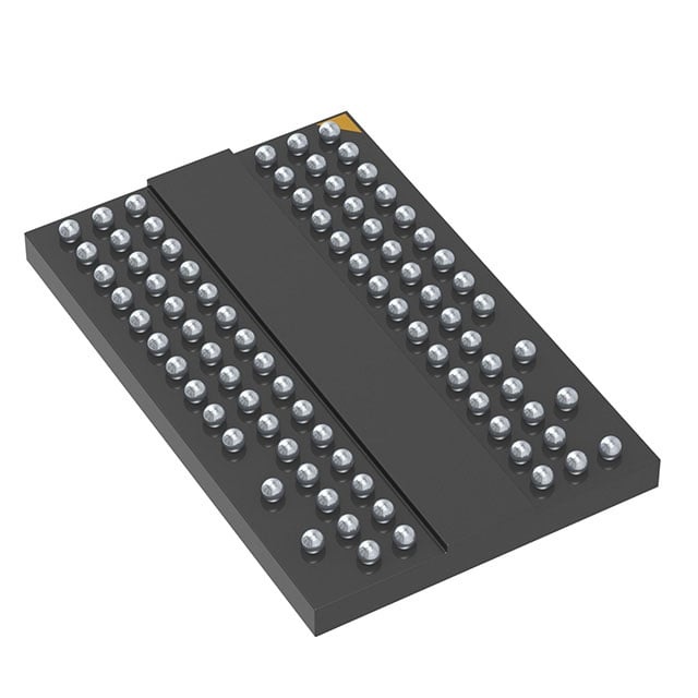
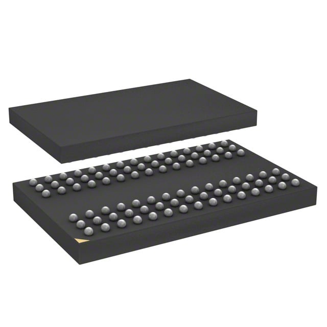
IC DRAM 128MBIT PAR 90TFBGA |
|---|---|
| Quantity | 556 Available (as of June 15, 2026) |

| Product Category | Memory |
|---|---|
| Manufacturer | Winbond Electronics |
| Manufacturing Status | Active |
| Manufacturer Standard Lead Time | 24 Weeks |
| Datasheet |
Specifications & Environmental
| Device Package | 90-TFBGA (8x13) | Memory Format | DRAM | Technology | SDRAM | ||
|---|---|---|---|---|---|---|---|
| Memory Size | 128 Mbit | Access Time | 5 ns | Grade | Commercial | ||
| Clock Frequency | 166 MHz | Voltage | 3V ~ 3.6V | Memory Type | Volatile | ||
| Operating Temperature | 0°C ~ 70°C (TA) | Write Cycle Time Word Page | N/A | Packaging | 90-TFBGA | ||
| Mounting Method | Volatile | Memory Interface | Parallel | Memory Organization | 4M x 32 | ||
| Moisture Sensitivity Level | 3 (168 Hours) | RoHS Compliance | ROHS3 Compliant | REACH Compliance | REACH Unaffected | ||
| Qualification | N/A | ECCN | EAR99 | HTS Code | 8542.32.0002 |
Overview of W9812G2KB-6 TR – IC DRAM 128Mbit PAR 90TFBGA
The W9812G2KB-6 TR from Winbond Electronics is a 128 Mbit synchronous DRAM (SDRAM) device organized as 1M × 4 banks × 32 bits (4M × 32). It implements a parallel SDRAM interface operating up to 166 MHz and supports burst-oriented access for sequential memory reads and writes.
This device targets designs that require compact parallel DRAM in a 90‑TFBGA (8×13) package and operate within a 3.0 V to 3.6 V supply range and 0 °C to 70 °C ambient temperature.
Key Features
- Memory Type Volatile SDRAM with burst-oriented access and support for burst lengths including 1, 2, 4, 8 or full page as described in the device functional description.
- Density & Organization 128 Mbit total capacity organized as 1M × 4 banks × 32 bits (4M × 32).
- Performance Clock frequency up to 166 MHz with specified CAS latency behavior referenced in the datasheet; typical access timing examples and read/write timing diagrams are provided.
- Access Time Access time listed as 5 ns in the device specifications.
- Voltage Supply Operates from 3.0 V to 3.6 V DC supply.
- Package 90‑TFBGA (8×13) ball grid array package for compact board footprint and high pin density.
- Operating Temperature Commercial temperature range specified as 0 °C to 70 °C (TA).
- Command & Power Modes Supports standard SDRAM command set including mode register set, bank activate, auto‑precharge, self‑refresh, power down and no‑operation commands as documented in the datasheet.
Typical Applications
- Embedded memory expansion Provides 128 Mbit of parallel SDRAM for embedded systems that require burst-capable volatile storage at up to 166 MHz.
- Board-level DRAM replacement Compact 90‑TFBGA footprint for designs needing a high-density SDRAM device in a small package.
- High-throughput buffering Banked 1M × 4 organization and burst access support use as a buffer memory where sequential read/write bursts are required.
Unique Advantages
- Parallel SDRAM interface: Direct parallel memory interface for designs that use standard SDRAM signaling and command sequences.
- Banked architecture: 1M × 4 banks × 32 bits organization enables interleaved bank operations and burst transfers documented in the datasheet timing examples.
- Compact BGA package: 90‑TFBGA (8×13) package provides high pin count in a small board area for space-constrained applications.
- Documented timing and command behavior: Comprehensive datasheet sections for operation modes, timing waveforms and example cycles (read/write, refresh, self‑refresh) simplify integration and verification.
- Standard voltage range: 3.0 V to 3.6 V supply range compatible with systems using standard 3.3 V power rails.
Why Choose W9812G2KB-6 TR?
The W9812G2KB-6 TR is positioned as a compact, parallel SDRAM solution delivering 128 Mbit capacity with a banked 1M × 4 × 32 organization and support for burst-oriented transfers up to a 166 MHz clock. Its documented command set, timing diagrams and operational examples help system designers integrate and validate memory behavior for buffering and sequential-access use cases.
This device is appropriate for designs requiring a 90‑TFBGA package, standard 3.0 V–3.6 V supply and commercial temperature operation (0 °C to 70 °C). The included datasheet material on power-up, initialization, power modes and timing provides the technical detail needed for engineering evaluation and system integration.
If you would like pricing, availability or a formal quote for W9812G2KB-6 TR, please request a quote or submit an RFQ to receive commercial terms and lead‑time information.