W9812G6JH-5
| Part Description |
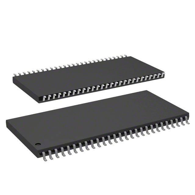
IC DRAM 128MBIT PAR 54TSOP II |
|---|---|
| Quantity | 24 Available (as of June 14, 2026) |
| Product Category | Memory |
|---|---|
| Manufacturer | Winbond Electronics |
| Manufacturing Status | Obsolete |
| Manufacturer Standard Lead Time | Contact Us |
| Datasheet |
Specifications & Environmental
| Device Package | 54-TSOP II | Memory Format | DRAM | Technology | SDRAM | ||
|---|---|---|---|---|---|---|---|
| Memory Size | 128 Mbit | Access Time | 4.5 ns | Grade | Commercial | ||
| Clock Frequency | 200 MHz | Voltage | 3V ~ 3.6V | Memory Type | Volatile | ||
| Operating Temperature | 0°C ~ 70°C (TA) | Write Cycle Time Word Page | N/A | Packaging | 54-TSOP (0.400", 10.16mm Width) | ||
| Mounting Method | Volatile | Memory Interface | Parallel | Memory Organization | 8M x 16 | ||
| Moisture Sensitivity Level | 3 (168 Hours) | RoHS Compliance | ROHS Compliant | REACH Compliance | REACH Unaffected | ||
| Qualification | N/A | ECCN | EAR99 | HTS Code | 8542.32.0002 |
Overview of W9812G6JH-5 – 128 Mbit Parallel SDRAM, 54‑TSOP II
The W9812G6JH-5 is a high-speed synchronous DRAM (SDRAM) device organized as 2M × 4 banks × 16 bits, providing a total density of 128 Mbit. The device implements a parallel SDRAM interface and is offered in a 54‑lead TSOP II package optimized for board-level integration.
Designed to operate at a clock frequency up to 200 MHz (‑5 grade, 200 MHz/CL3), the device targets systems requiring synchronous parallel DRAM with burst read/write support, standard SDRAM command sets, and a 3.0 V to 3.6 V supply range.
Key Features
- Memory organization and density 128 Mbit SDRAM organized as 8M × 16 with internal configuration of 2M × 4 banks × 16 bits for efficient bank and page access.
- Synchronous SDRAM core High-speed synchronous DRAM architecture with standard SDRAM command set including bank activate, read/write, auto-precharge and refresh operations.
- Performance Qualified for the -5 speed grade at up to 200 MHz and compliant to 200 MHz/CL3 timing; typical access time listed as 4.5 ns.
- Burst and addressing modes Supports burst read/write operations and multiple addressing sequences (sequential and interleave) to optimize throughput.
- Power and low-power modes Includes self-refresh, auto-refresh and power-down commands to manage power during idle and retention states.
- Voltage and temperature Operates from 3.0 V to 3.6 V with an ambient operating temperature range of 0 °C to 70 °C (TA).
- Package Available in a 54‑TSOP II package (0.400", 10.16 mm width) for compact board-level mounting.
Typical Applications
- PC-standard memory subsystems Designs that require SDRAM timing compliant with PC-standard specifications (200 MHz/CL3) can use this part for synchronous parallel memory.
- Board-level SDRAM implementations Systems requiring a 54‑TSOP II footprint for compact integration and parallel SDRAM connectivity.
- Embedded systems with parallel memory interfaces Applications that need 128 Mbit of parallel SDRAM and standard SDRAM command/mode support for burst or page-mode transfers.
Unique Advantages
- Deterministic timing at 200 MHz (‑5) The -5 grade is specified to meet 200 MHz/CL3 timing, supporting predictable SDRAM timing for synchronous designs.
- Flexible bank and burst architecture 2M × 4 banks × 16-bit organization plus burst modes enable efficient multi-word transfers and interleaved bank access.
- Standard SDRAM command set Built-in support for mode register set, auto-precharge, self-refresh, power-down and other standard commands simplifies controller design.
- 3.0–3.6 V compatibility Supports common 3.3 V nominal supply rails used in many parallel memory systems.
- Space-efficient package 54‑lead TSOP II package (0.400", 10.16 mm) for compact PCB implementations where a parallel SDRAM footprint is required.
- Documented timing and operation Detailed datasheet coverage of power-up, mode programming, timing waveforms and operating examples to aid integration and validation.
Why Choose W9812G6JH-5?
The W9812G6JH-5 delivers a synchronous parallel DRAM solution with 128 Mbit density, standard SDRAM command support and 200 MHz/CL3 timing in a compact 54‑TSOP II package. Its banked architecture and burst modes provide designers with efficient data transfer options for systems that require deterministic SDRAM timing and parallel interface integration.
This device is suited to designers and OEMs implementing board-level parallel SDRAM where a 3.0–3.6 V supply, 0 °C to 70 °C operating range, and documented SDRAM behavior (mode registers, refresh, self-refresh and power-down) are required for reliable system integration.
Request a quote or contact sales to discuss availability, pricing, and technical support for W9812G6JH-5.