W9825G2JB-75 TR
| Part Description |
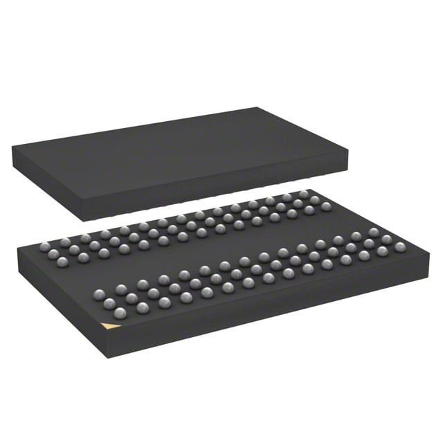
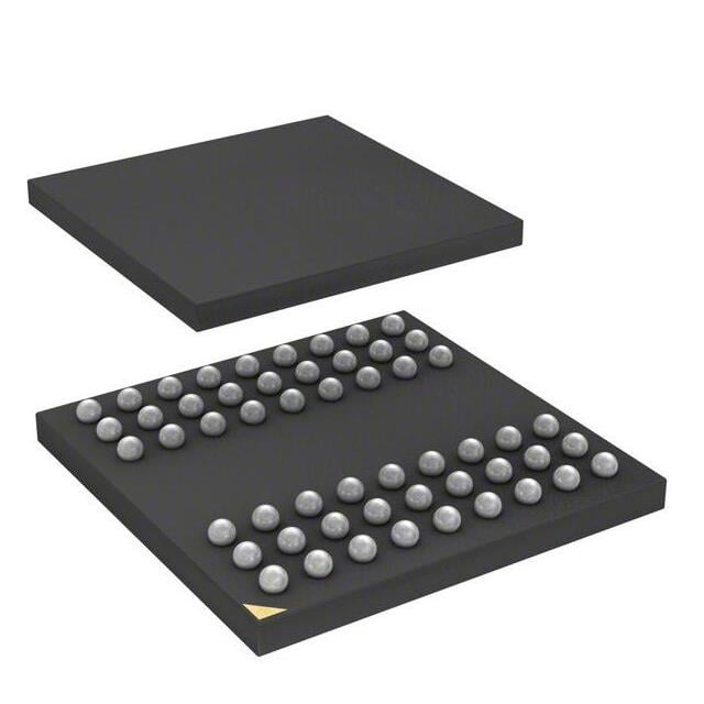
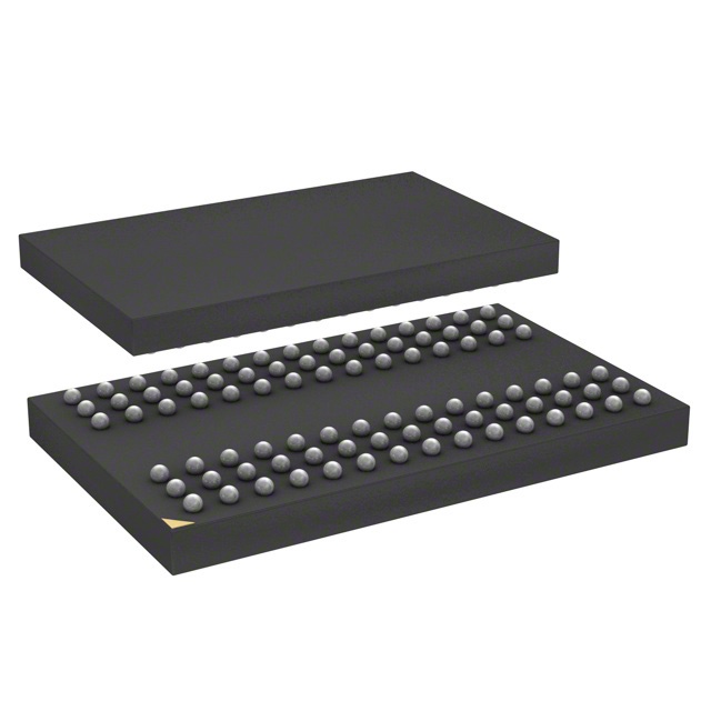
IC DRAM 256MBIT PAR 90TFBGA |
|---|---|
| Quantity | 83 Available (as of June 14, 2026) |

| Product Category | Memory |
|---|---|
| Manufacturer | Winbond Electronics |
| Manufacturing Status | Obsolete |
| Manufacturer Standard Lead Time | Contact Us |
| Datasheet |
Specifications & Environmental
| Device Package | 90-TFBGA (8x13) | Memory Format | DRAM | Technology | SDRAM | ||
|---|---|---|---|---|---|---|---|
| Memory Size | 256 Mbit | Access Time | 5.4 ns | Grade | Commercial | ||
| Clock Frequency | 133 MHz | Voltage | 3V ~ 3.6V | Memory Type | Volatile | ||
| Operating Temperature | 0°C ~ 70°C (TA) | Write Cycle Time Word Page | N/A | Packaging | 90-TFBGA | ||
| Mounting Method | Volatile | Memory Interface | Parallel | Memory Organization | 16M x 16 | ||
| Moisture Sensitivity Level | 3 (168 Hours) | RoHS Compliance | ROHS3 Compliant | REACH Compliance | REACH Unaffected | ||
| Qualification | N/A | ECCN | EAR99 | HTS Code | 8542.32.0024 |
Overview of W9825G2JB-75 TR – IC DRAM 256Mbit PAR 90TFBGA
The W9825G2JB-75 TR is a 256 Mbit volatile SDRAM device organized as 16M × 16 with a parallel memory interface. It provides high-speed synchronous DRAM functionality with specified timing and power characteristics for system memory integration.
This device targets designs requiring 256 Mbit of parallel SDRAM operating at up to 133 MHz with a 3.0 V–3.6 V supply and an ambient operating range of 0°C to 70°C (TA).
Key Features
- Memory Type & Architecture Volatile SDRAM organized as 16M × 16 (256 Mbit) with a parallel memory interface.
- Density 256 Mbit total memory capacity.
- Performance Specified clock frequency of 133 MHz and an access time of 5.4 ns; the -75 speed grade is compliant to the 133 MHz / CL3 specification as noted in the product documentation.
- Standard SDRAM Operations Supports standard SDRAM command set and modes such as bank activate, burst read/write, auto-precharge, self-refresh and power-down (described in the device documentation).
- Power Supply voltage range: 3.0 V to 3.6 V.
- Package 90‑TFBGA package (8 × 13 ball array) for compact board-level mounting.
- Operating Temperature Rated for ambient temperatures from 0°C to 70°C (TA).
Unique Advantages
- Clear performance specification: Clock frequency (133 MHz) and access time (5.4 ns) give predictable timing for memory subsystem design and timing budgets.
- Compact BGA footprint: 90‑TFBGA (8×13) packaging reduces board area while maintaining a parallel interface for straightforward routing.
- Standard SDRAM command support: Documentation details standard SDRAM commands and modes (burst read/write, auto-precharge, self-refresh, power-down), simplifying integration into existing SDRAM controllers.
- <strong-Wide supply tolerance: Operates across a 3.0 V–3.6 V supply range to accommodate typical 3.3 V system rails.
- Verified speed grade: The -75 speed grade is specified for operation at the 133 MHz / CL3 timing point documented for the device.
Why Choose W9825G2JB-75 TR?
The W9825G2JB-75 TR provides a concise specification set for designers needing a 256 Mbit parallel SDRAM with defined timing (133 MHz, 5.4 ns access) and standard SDRAM operational modes. Its 90‑TFBGA package and 3.0 V–3.6 V supply range make it suitable for compact board-level memory applications where a parallel SDRAM interface and predictable timing are required.
This device is appropriate for engineers and procurement teams looking for a documented SDRAM option with clear electrical, timing and package data to support system memory design and validation.
Request a quote or submit a product inquiry to receive pricing and availability information for the W9825G2JB-75 TR.