W9825G2JB-75
| Part Description |
IC DRAM 256MBIT PAR 90TFBGA |
|---|---|
| Quantity | 817 Available (as of June 15, 2026) |

| Product Category | Memory |
|---|---|
| Manufacturer | Winbond Electronics |
| Manufacturing Status | Obsolete |
| Manufacturer Standard Lead Time | Contact Us |
| Datasheet |
Specifications & Environmental
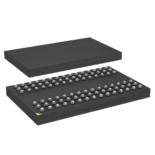
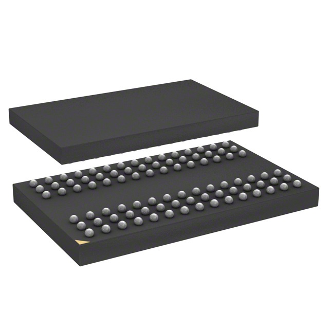
| Device Package | 90-TFBGA (8x13) | Memory Format | DRAM | Technology | SDRAM | ||
|---|---|---|---|---|---|---|---|
| Memory Size | 256 Mbit | Access Time | 5.4 ns | Grade | Commercial | ||
| Clock Frequency | 133 MHz | Voltage | 3V ~ 3.6V | Memory Type | Volatile | ||
| Operating Temperature | 0°C ~ 70°C (TA) | Write Cycle Time Word Page | N/A | Packaging | 90-TFBGA | ||
| Mounting Method | Volatile | Memory Interface | Parallel | Memory Organization | 16M x 16 | ||
| Moisture Sensitivity Level | 3 (168 Hours) | RoHS Compliance | ROHS3 Compliant | REACH Compliance | REACH Unaffected | ||
| Qualification | N/A | ECCN | EAR99 | HTS Code | 8542.32.0002 |
Overview of W9825G2JB-75 – IC DRAM 256MBIT PAR 90TFBGA
The W9825G2JB-75 is a 256 Mbit synchronous dynamic RAM (SDRAM) device organized as 16M × 16 (4M × 4 banks × 16 bits). It provides a parallel SDRAM interface in a compact 90‑TFBGA (8×13) package and is specified for operation at a 133 MHz clock frequency with a 5.4 ns access time.
This device is designed for use where a parallel SDRAM memory element with defined voltage and temperature ranges is required. Key electrical parameters include a supply voltage range of 3.0 V to 3.6 V and an operating ambient temperature range of 0°C to 70°C.
Key Features
- Memory Type & Architecture 256 Mbit SDRAM organized as 16M × 16 (4M × 4 banks × 16 bits), supporting burst-oriented access.
- Performance Specified for a 133 MHz clock frequency with a 5.4 ns access time to meet mid‑range synchronous memory timing.
- Interface Parallel SDRAM interface suitable for systems that require conventional DRAM bus signaling.
- Voltage Supply Operates from 3.0 V to 3.6 V, enabling compatibility with standard 3.3 V system rails.
- Package 90‑TFBGA (8×13) supplier device package for a small-footprint, surface-mount implementation.
- Operating Temperature Rated for 0°C to 70°C (TA), appropriate for commercial temperature-range applications.
Typical Applications
- Parallel memory expansion — Provides 256 Mbit of SDRAM in a 16M × 16 organization for systems requiring parallel DRAM.
- Embedded systems — Compact 90‑TFBGA package and standard voltage range support space-constrained board designs using a 3.3 V rail.
- Mid-performance synchronous memory — 133 MHz operation and 5.4 ns access time for designs that need deterministic SDRAM timing.
Unique Advantages
- High-density SDRAM — 256 Mbit capacity in a single device reduces component count for designs needing larger DRAM arrays.
- Standard parallel SDRAM architecture — 16M × 16 organization with multiple banks supports burst-oriented access patterns.
- Compact BGA package — 90‑TFBGA (8×13) packaging minimizes PCB footprint while providing a robust surface-mount solution.
- System-level compatibility — 3.0 V to 3.6 V supply and 133 MHz clock support integration with common 3.3 V systems and SDRAM controllers.
- Commercial temperature rating — 0°C to 70°C ambient operating range for standard commercial applications.
Why Choose W9825G2JB-75?
The W9825G2JB-75 delivers a straightforward, high-density SDRAM option with a parallel interface, predictable timing (133 MHz / 5.4 ns access), and a compact 90‑TFBGA footprint. Its 16M × 16 organization (4M × 4 banks × 16 bits) and 3.0 V to 3.6 V supply range make it suitable for designs that require a conventional SDRAM element with defined electrical and temperature specifications.
This device is well suited for engineers and procurement teams specifying memory for systems that need mid-range synchronous DRAM capacity and performance while keeping board area and BOM count minimized.
Request a quote or submit a pricing inquiry to learn more about availability, lead times, and ordering options for the W9825G2JB-75.