
LX2120SE72029B
| Part Description |
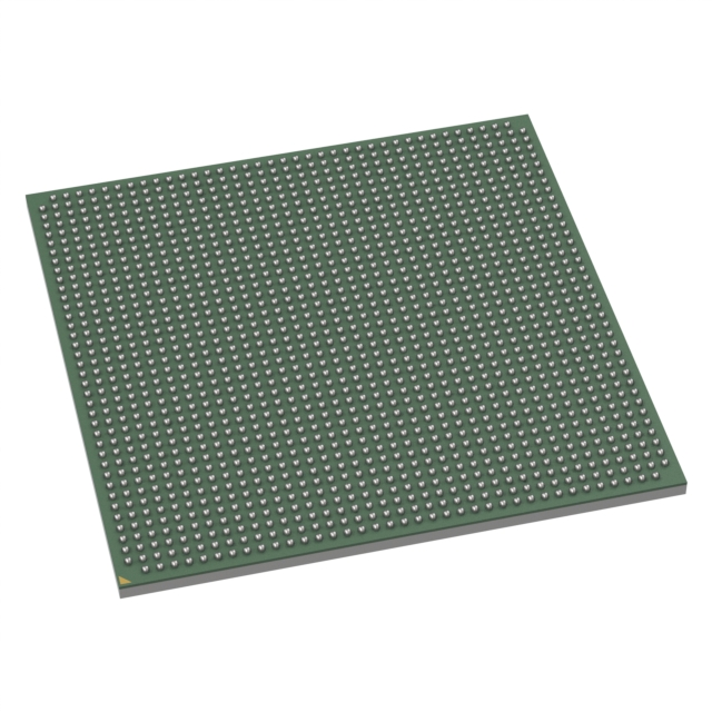
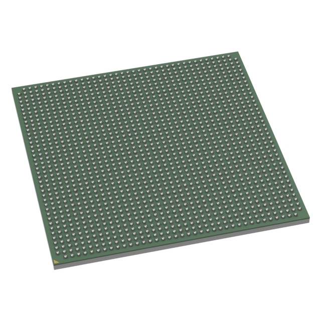
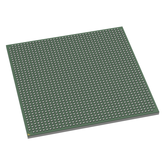
ARM® Cortex®-A72 Microprocessor IC QorlQ LX2 12 Core, 64-Bit 2GHz 1517-FCPBGA (40x40) |
|---|---|
| Quantity | 11 Available (as of October 8, 2026) |
| Product Category | Microprocessors |
|---|---|
| Part Series | LX2120S |
| Manufacturer | NXP USA Inc. |
| Manufacturing Status | Active |
| Manufacturer Standard Lead Time | 18 Weeks |
| Datasheet |
Specifications & Environmental
| Core Processor | ARM® Cortex®-A72 | Device Package | 1517-FCPBGA (40x40) | ECCN | N/A | ||
|---|---|---|---|---|---|---|---|
| Ethernet | 100Gbps (2) | Graphics Acceleration | Yes | HTS Code | N/A | ||
| Moisture Sensitivity Level | N/A | Mounting Method | Surface Mount | Mounting Type | Surface Mount | ||
| Number of Cores/Bus Width | 12 Core, 64-Bit | Operating Temperature | 0°C ~ 105°C (TJ) | Package / Case | 1517-BBGA, FCBGA | ||
| RAM Controllers | DDR4 | REACH Compliance | REACH Unaffected | RoHS Compliance | ROHS3 Compliant | ||
| SATA | SATA 3.0 (4) | Security Features | Secure Boot, TrustZone® | Speed | 2GHz | ||
| Supplier Device Package | 1517-FCPBGA (40×40) | USB | USB 3.0 (2) + PHY (2) | Voltage – I/O | 1.2V, 1.8V, 3.3V |
Overview of LX2120SE72029B – IC MPU QORLQ LX2 2GHZ 1517FCPBGA
The LX2120SE72029B from NXP Semiconductors is a 12-core, 64-bit ARM® Cortex®-A72 microprocessor in the Layerscape LX2120S family. Running at up to 2 GHz, this high-performance MPU combines multi-core processing and rich I/O to address compute-intensive networking, edge processing, data-center offload and 5G packet-processing applications.
Designed for embedded and networking platforms, the device emphasizes integration and throughput with high-speed Ethernet, multiple storage and peripheral interfaces, and built-in security features to support secure boot and trusted execution environments.
Key Features
- Core/CPU 12 × ARM® Cortex®-A72 64‑bit cores running up to 2 GHz for multi-threaded, compute-intensive workloads.
- Memory DDR4 memory controller support (as specified) for high-bandwidth external memory configurations.
- High‑Speed Ethernet Two 100 Gbps Ethernet ports enabling high-throughput network connectivity for data‑plane and control‑plane tasks.
- Storage Interfaces Four SATA 3.0 ports for multiple high-speed storage connections.
- USB and PHY Two USB 3.0 ports plus two USB PHY interfaces for modern peripheral and host connectivity.
- Peripheral Buses CANbus support for robust in‑vehicle or industrial control networking and general-purpose serial I/O.
- Security Secure Boot and Arm TrustZone® support to enable trusted boot flows and hardware-isolated execution.
- Graphics Acceleration Integrated graphics acceleration to support display or graphics‑offload tasks.
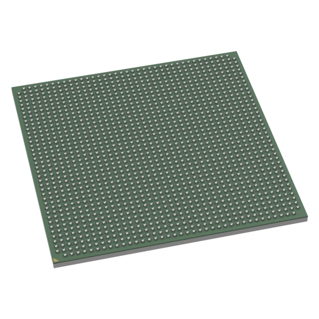
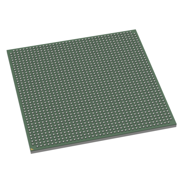
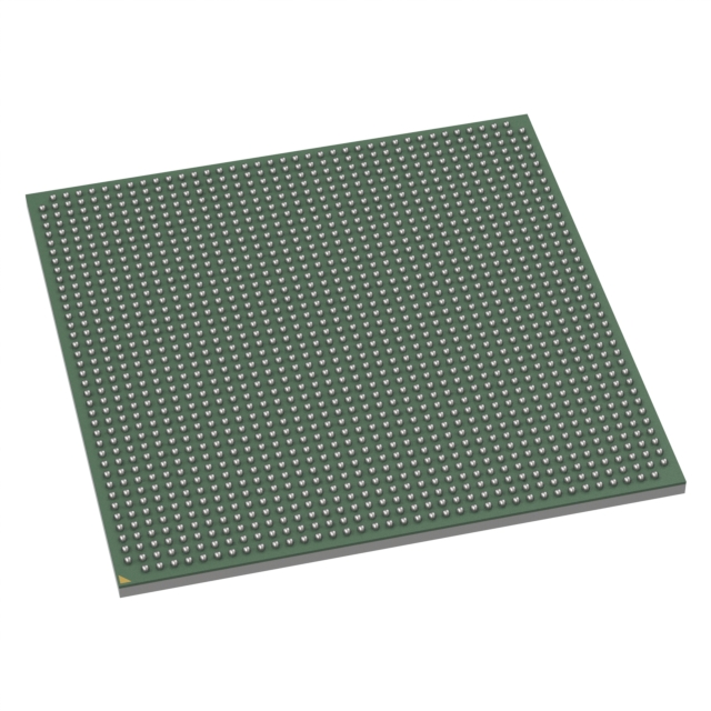
- Package & Mounting 1517‑FCPBGA (40 × 40) surface‑mount FCBGA package for compact board integration.
- Operating Temperature Rated for 0 °C to 105 °C to cover a broad range of embedded operating environments.
- RoHS RoHS‑compliant construction.
Typical Applications
- Networking Infrastructure — High-throughput routing, switching and control-plane functions leveraging dual 100 Gbps Ethernet ports.
- Edge and Data‑Center Offload — Compute and packet-processing tasks that benefit from multi-core CPU performance and onboard acceleration.
- 5G Packet Processing — Baseband and packet‑processing functions that require multi-core processing and high network bandwidth.
- Industrial Connectivity — Gateways and controllers that use CANbus, multiple storage interfaces and broad temperature operation.
Unique Advantages
- Multi‑core Performance: Twelve Cortex‑A72 cores at up to 2 GHz provide parallel compute resources for packet processing and application hosting.
- High‑bandwidth Networking: Two 100 Gbps Ethernet ports enable sustained, wire‑rate data movement for demanding network applications.
- Comprehensive I/O Set: Integrated SATA, USB, CAN and PHY interfaces reduce external bridge requirements and simplify BOM.
- Hardware Security: Secure Boot and TrustZone® support help protect boot integrity and run-time secrets without external processors.
- Compact, Surface‑Mount Package: 1517‑FCPBGA (40×40) enables dense board designs while providing a robust thermal footprint.
- Vendor Software Ecosystem: Layerscape family tooling and SDKs are available to support development and deployment.
Why Choose LX2120SE72029B?
The LX2120SE72029B balances multi‑core compute performance with rich, high‑speed I/O and hardware security primitives, making it well suited for embedded networking and edge compute designs. Its combination of 12 ARM® Cortex®‑A72 cores, dual 100 Gbps Ethernet connectivity, multiple storage and peripheral interfaces, and a compact FCBGA package helps reduce system complexity while delivering the throughput required for modern networked applications.
Backed by NXP Semiconductors and the Layerscape family ecosystem, this MPU is appropriate for developers seeking a scalable, integrated platform for networking, 5G packet processing, data‑center offload and industrial connectivity solutions.
Request a quote or submit a purchase inquiry to get pricing, availability and lead‑time information for the LX2120SE72029B.



















Date Founded: 2006
Headquarters: Eindhoven, North Brabant, Netherlands
Employees: 38,000+
Revenue: $10.53 Billion
Certifications and Memberships: ISO9001:2015, IATF16949:2016


