
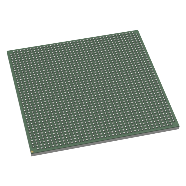
LX2160XN71826B
| Part Description |
ARM® Cortex®-A72 Microprocessor IC QorlQ LX2 16 Core, 64-Bit 1.8GHz 1517-FCPBGA (40x40) |
|---|---|
| Quantity | 981 Available (as of October 8, 2026) |
| Product Category | Microprocessors |
|---|---|
| Part Series | LX2160X |
| Manufacturer | NXP USA Inc. |
| Manufacturing Status | Active |
| Manufacturer Standard Lead Time | 18 Weeks |
| Datasheet |
Specifications & Environmental
| Core Processor | ARM® Cortex®-A72 | Device Package | 1517-FCPBGA (40x40) | ECCN | 3A991A2 | ||
|---|---|---|---|---|---|---|---|
| Ethernet | 100Gbps (2) | Graphics Acceleration | Yes | HTS Code | 8542.31.0001 | ||
| Moisture Sensitivity Level | N/A | Mounting Method | Surface Mount | Mounting Type | Surface Mount | ||
| Number of Cores/Bus Width | 16 Core, 64-Bit | Operating Temperature | -40°C ~ 105°C (TJ) | Package / Case | 1517-BBGA, FCBGA | ||
| RAM Controllers | DDR4 | REACH Compliance | REACH Unaffected | RoHS Compliance | ROHS3 Compliant | ||
| SATA | SATA 3.0 (4) | Security Features | Secure Boot, TrustZone® | Speed | 1.8GHz | ||
| Supplier Device Package | 1517-FCPBGA (40×40) | USB | USB 3.0 (2) + PHY (2) | Voltage – I/O | 1.2V, 1.8V, 3.3V |
Overview of LX2160XN71826B – IC MPU QORLQ 1.8GHZ 1517FCPBGA
The LX2160XN71826B is an NXP Layerscape QorlQ microprocessor IC based on 16 Arm® Cortex®-A72 64-bit cores running at 1.8 GHz. It targets compute‑intensive embedded and networking applications, delivering high integration for packet processing, security offload, and edge/industrial processing while maintaining a compact FCPBGA footprint.
Designed for systems requiring high throughput and robust I/O, this device combines multi‑core compute with accelerated security, compression, and a broad set of interfaces to simplify board design and reduce external component needs.
Key Features
- Core & Architecture Sixteen 64‑bit Arm® Cortex®‑A72 CPU cores clocked at 1.8 GHz, providing parallel compute for control and data‑plane tasks.
- Memory & Caching Dual DDR4 controllers with ECC support and on‑chip caching; datasheet references up to 2 × DDR4 72b and a 16 MB cache plus a 2 MB packet caching buffer to reduce external memory traffic.
- Security & Acceleration Integrated secure boot and Arm TrustZone® security features, plus hardware accelerators cited for up to 50 Gbit/s security offload and 100 Gbit/s compression/decompression.
- High‑Speed Connectivity Dual 100 Gbit/s Ethernet capability and a 122 Gbit/s Layer‑2 switch architecture, with up to 16 supported Ethernet ports for dense network interfaces.
- SerDes & PCIe High‑speed SerDes lane support (24 lanes up to 25 GHz) and up to 24 PCIe Gen3 lanes supporting multiple ports, enabling flexible host and NIC connectivity.
- Storage & Peripherals Four SATA 3.0 ports, two USB 3.0 ports (plus two USB PHYs), SD/eMMC, DUART, I2C and CAN interfaces for broad peripheral support.
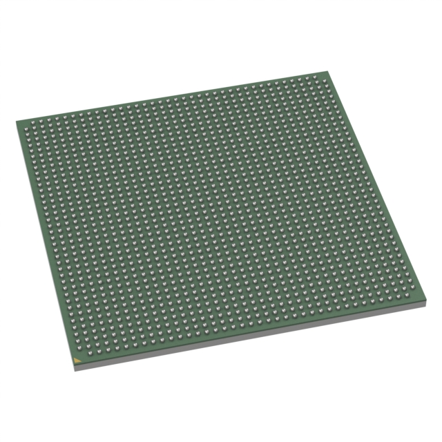
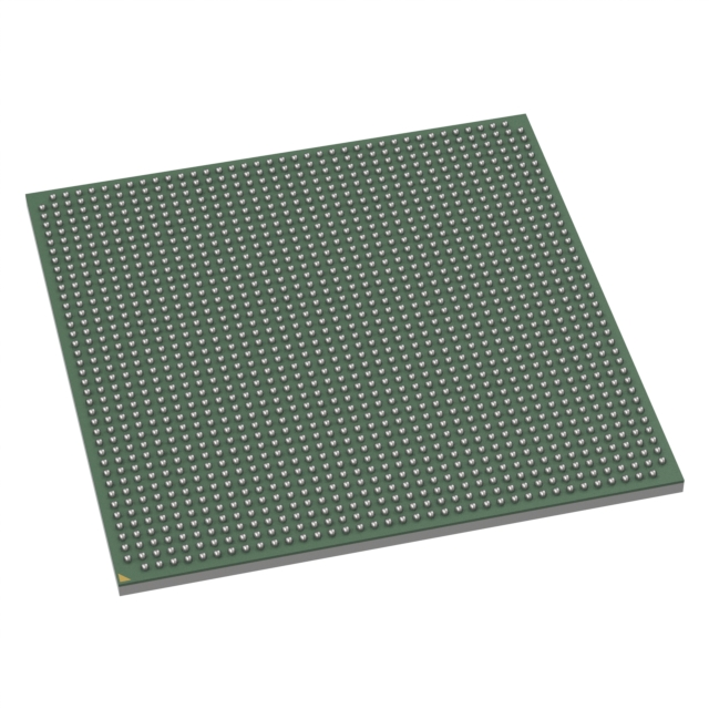
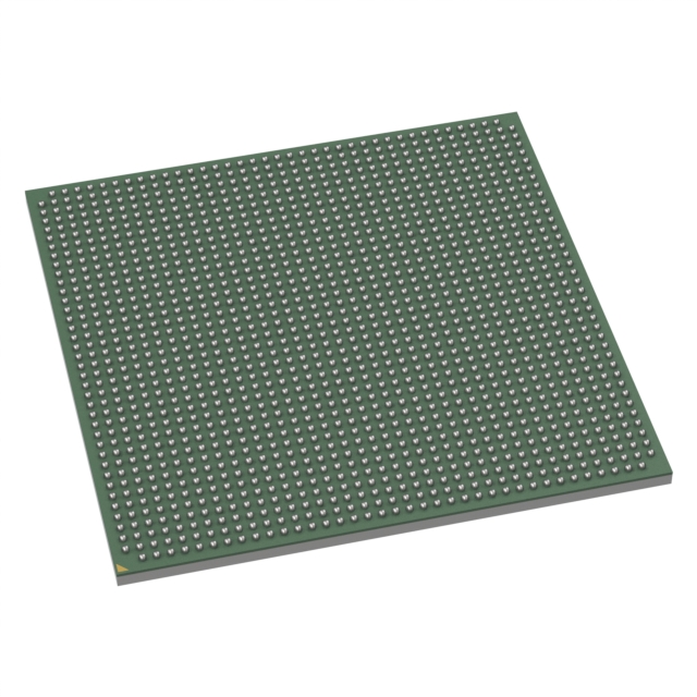
- Package & Mounting 1517‑FCPBGA (40 × 40 mm) FCBGA package for surface‑mount applications, suitable for compact embedded designs.
- Operating Range & Compliance Industrial qualification with operating temperature from −40 °C to 105 °C and RoHS compliance for environmental compatibility.
- Graphics & Offload Graphics acceleration supported and dedicated engines for packet and data handling to offload host cores.
Typical Applications
- Network Appliances: Control and data‑plane processing, including switches and routers that require high Ethernet throughput and hardware offload.
- White‑Box Switching / Edge Compute: Host virtualization and edge processing with dense I/O, leveraging integrated MACs, PCIe, and packet caching.
- Data Center Offload: Acceleration of IPsec, compression, and other compute‑intensive networking functions to reduce host CPU load.
- 5G Packet Processing: Packet throughput and security/compression offload in distributed unit and central unit applications.
- Industrial Edge Systems: Embedded control and connectivity hubs that benefit from broad peripheral interfaces, extended temperature range, and ECC DDR4 memory support.
Unique Advantages
- Highly integrated compute and I/O: Sixteen Arm® Cortex®‑A72 cores with extensive SerDes, PCIe, Ethernet and peripheral sets reduce board complexity and BOM.
- Hardware offload engines: Dedicated security and compression accelerators enable higher throughput with lower host CPU utilization.
- Packet‑aware caching: On‑chip packet cache minimizes external memory dependence for lower latency and reduced power in packet processing workloads.
- Industrial ready: Industrial qualification and −40 °C to 105 °C operating range support demanding embedded deployments.
- Compact FCBGA package: 1517‑FCPBGA (40×40) package enables dense board integration for constrained spaces.
- Long portfolio support: Layerscape family software ecosystem including Linux SDK and CodeWarrior support aids development and long‑term maintenance.
Why Choose LX2160XN71826B?
The LX2160XN71826B combines multi‑core Arm® Cortex®‑A72 performance with broad, high‑speed I/O and dedicated offload engines, making it a strong choice for developers building high‑throughput networking, edge compute, and industrial applications. Its integrated feature set—DDR4 with ECC, dual 100 Gbit/s Ethernet capability, SerDes/PCIe flexibility, and security/compression accelerators—reduces external components and simplifies system architecture.
For designs that demand scalable performance, robust I/O, and industrial temperature operation, this device offers a balanced platform with an established Layerscape software ecosystem to accelerate time‑to‑market and long‑term product support.
Request a quote or submit an inquiry for LX2160XN71826B to receive pricing and availability information and to discuss lead time and volume options.



















Date Founded: 2006
Headquarters: Eindhoven, North Brabant, Netherlands
Employees: 38,000+
Revenue: $10.53 Billion
Certifications and Memberships: ISO9001:2015, IATF16949:2016


