
MPC8270ZUQLDA
| Part Description |
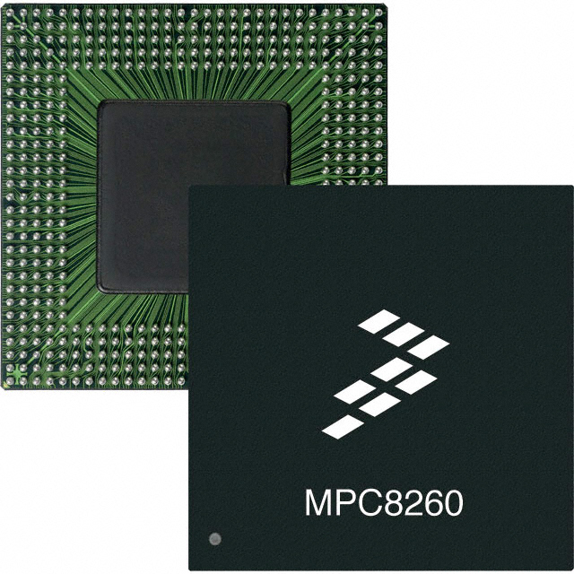
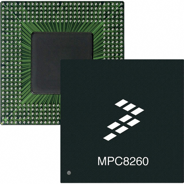
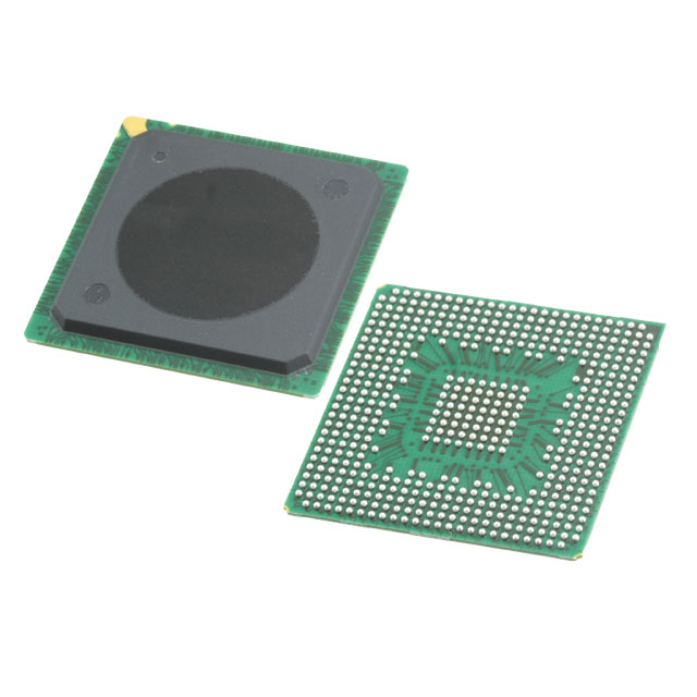
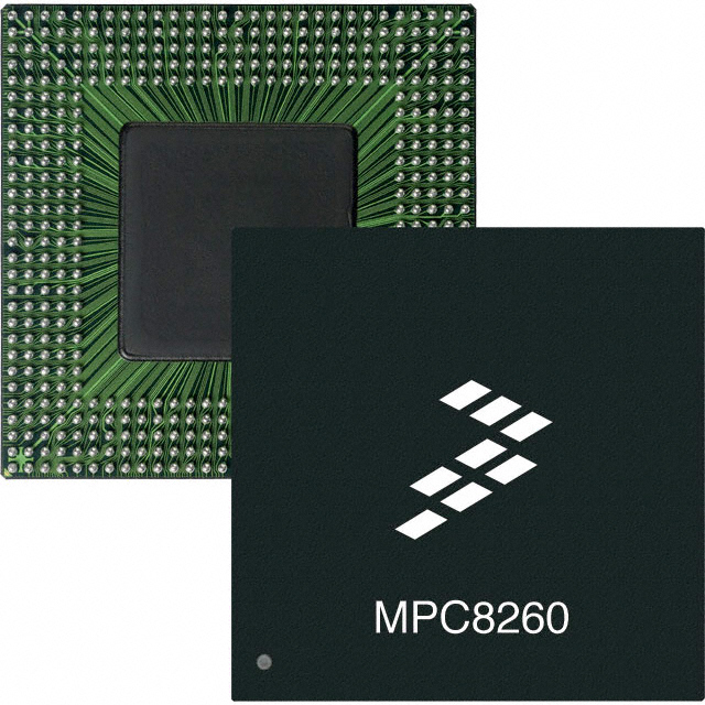
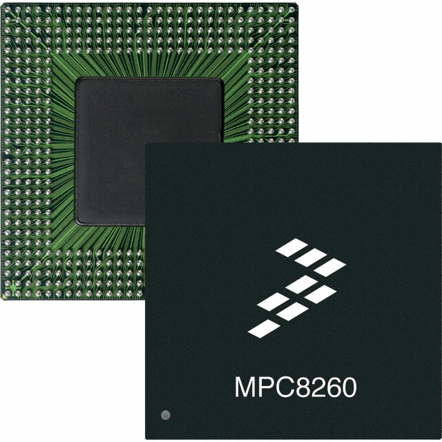
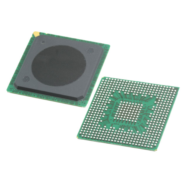
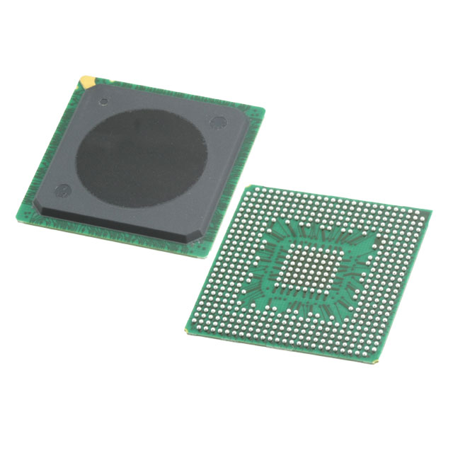
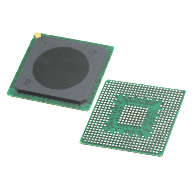
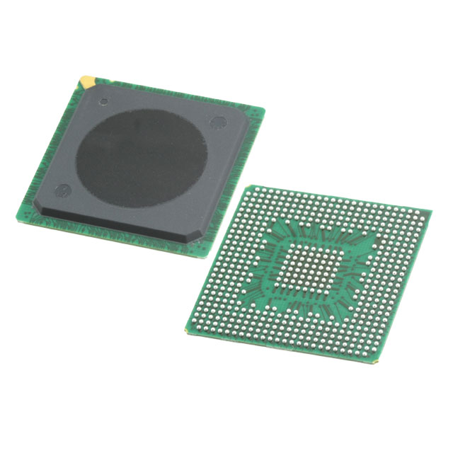
PowerPC G2_LE Microprocessor IC MPC82xx 1 Core, 32-Bit 333MHz 480-TBGA (37.5x37.5) |
|---|---|
| Quantity | 287 Available (as of October 8, 2026) |
| Product Category | Microprocessors |
|---|---|
| Part Series | MPC8270 |
| Manufacturer | NXP USA Inc. |
| Manufacturing Status | Obsolete |
| Manufacturer Standard Lead Time | Contact Us |
| Datasheet |
Specifications & Environmental
| Co-Processors/DSP | Communications; RISC CPM | Core Processor | PowerPC G2_LE | Device Package | 480-TBGA (37.5x37.5) | ||
|---|---|---|---|---|---|---|---|
| ECCN | 5A991B4B | Ethernet | 10/100Mbps (3) | Graphics Acceleration | No | ||
| HTS Code | 8542.31.0001 | Moisture Sensitivity Level | 4 (72 Hours) | Mounting Method | Surface Mount | ||
| Mounting Type | Surface Mount | Number of Cores/Bus Width | 1 Core, 32-Bit | Operating Temperature | 0°C ~ 105°C (TA) | ||
| Package / Case | 480-LBGA Exposed Pad | RAM Controllers | DRAM, SDRAM | REACH Compliance | REACH Unaffected | ||
| RoHS Compliance | RoHS non-compliant | Speed | 333MHz | Supplier Device Package | 480-TBGA (37.5×37.5) | ||
| USB | USB 2.0 (1) | Voltage – I/O | 3.3V |
Overview of MPC8270ZUQLDA – IC MPU MPC82XX 333MHz 480-TBGA
The MPC8270ZUQLDA is a single‑core PowerPC G2_LE microprocessor designed for embedded communications and systems applications. The device integrates a 32‑bit PowerPC core running at 333 MHz with on‑chip controllers and peripheral interfaces to support networked and embedded designs.
Built for embedded and consumer applications, this NXP Semiconductors device emphasizes system integration—combining memory controllers, multiple Ethernet ports, USB, and serial communications controllers—to simplify board design and accelerate time to market.
Key Features
- Processor Core: PowerPC G2_LE 32‑bit core, single core running at 333 MHz, dual‑issue integer architecture as part of the PowerQUICC II family.
- Cache Architecture: Separate instruction and data caches with 16 KB I‑Cache and 16 KB D‑Cache (four‑way set associative, LRU replacement) as documented for the family.
- Communications Co‑processors: Integrated communications co‑processors including RISC CPM and serial communications controllers (SCCs) to support protocol handling and serial links.
- Memory Interfaces: On‑chip DRAM and SDRAM controllers for direct memory interfacing in embedded systems.
- Networking & USB: Three 10/100 Mbps Ethernet ports and one USB 2.0 full/low‑rate interface for networked and peripheral connectivity.
- System Integration: PCI bridge and multiple on‑chip controllers from the PowerQUICC II family to reduce external component count and simplify system design.
- Package & Mounting: 480‑TBGA (37.5×37.5 mm) package with exposed pad, surface‑mount mounting type suitable for high‑pin‑count board layouts.
- Electrical & Environmental: 3.3 V I/O voltage and RoHS‑compliant construction; consumer qualification.
- Operating Temperature: Rated for operation from 0 °C to 105 °C.
Typical Applications
- Embedded Networking Equipment: Multiple 10/100 Mbps Ethernet ports and on‑chip communications controllers enable gateways, routers, and network appliances with integrated protocol handling.
- Industrial and Control Systems: DRAM/SDRAM controllers and robust thermal range (0 °C to 105 °C) support embedded controllers and automation nodes operating within the specified temperature envelope.
- Communication Endpoints: Serial communications controllers and RISC CPM offload protocol tasks for managed switches, terminal adapters, and telecom‑adjacent communications devices.
- Embedded Consumer Products: Consumer‑qualified platform for connected devices that require integrated Ethernet, USB, and memory interfaces in a compact BGA package.
Unique Advantages
- Integrated Communications Peripherals: On‑chip Ethernet, USB and serial controllers reduce external IC count and simplify BOM and board routing.
- PowerQUICC II Family Architecture: Family‑level features such as a dual‑issue PowerPC core and documented cache architecture provide predictable performance characteristics for embedded workloads.
- High‑Density Package: 480‑TBGA (37.5×37.5) with exposed pad enables high pin count connectivity in a compact footprint for complex system designs.
- Direct Memory Support: Built‑in DRAM and SDRAM controllers streamline memory subsystem design and integration.
- Industry‑Standard I/O Voltage: 3.3 V I/O compatibility eases integration with common legacy and modern interfaces.
Why Choose MPC8270ZUQLDA?
The MPC8270ZUQLDA combines a PowerPC G2_LE single core at 333 MHz with extensive on‑chip communications and memory interfaces, positioning it as a practical choice for embedded and consumer communications designs that require integrated networking, serial, and memory support. Its family heritage within the PowerQUICC II series provides documented architecture and peripheral mappings to aid system design and verification.
This part is well suited for engineers seeking a compact, integrated processor solution from NXP Semiconductors for networked embedded systems, communication endpoints, and consumer‑grade products where consolidated I/O, Ethernet, USB, and memory interface capability reduce board complexity and accelerate development.
Request a quote or submit your requirements for the MPC8270ZUQLDA to receive pricing and availability information tailored to your design needs.





















Date Founded: 2006
Headquarters: Eindhoven, North Brabant, Netherlands
Employees: 38,000+
Revenue: $10.53 Billion
Certifications and Memberships: ISO9001:2015, IATF16949:2016


