
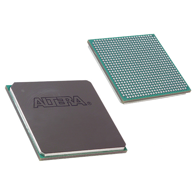
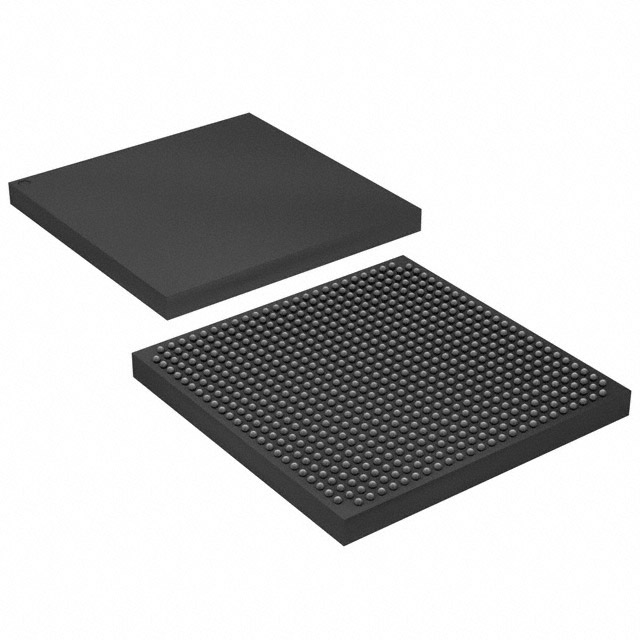
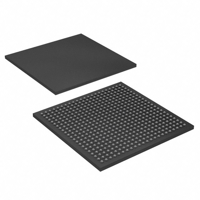
10AX022E3F27E1SG
| Part Description |
Arria 10 GX Field Programmable Gate Array (FPGA) IC 240 13752320 220000 672-BBGA, FCBGA |
|---|---|
| Quantity | 1,418 Available (as of June 15, 2026) |

| Product Category | Field Programmable Gate Array (FPGA) |
|---|---|
| Manufacturer | Intel |
| Manufacturing Status | Discontinued |
| Manufacturer Standard Lead Time | 13 Weeks |
| Datasheet |
Specifications & Environmental
| Device Package | 672-FBGA (27x27) | Grade | Extended | Operating Temperature | 0°C – 100°C | ||
|---|---|---|---|---|---|---|---|
| Package / Case | 672-BBGA, FCBGA | Number of I/O | 240 | Voltage | 870 mV - 930 mV | ||
| Mounting Method | Surface Mount | RoHS Compliance | RoHS Compliant | REACH Compliance | REACH Unaffected | ||
| Moisture Sensitivity Level | 3 (168 Hours) | Number of LABs/CLBs | 80330 | Number of Logic Elements/Cells | 220000 | ||
| Number of Gates | N/A | ECCN | 5A002A1 | HTS Code | 8542.39.0001 | ||
| Qualification | N/A | Total RAM Bits | 13752320 |
Overview of 10AX022E3F27E1SG – Arria 10 GX FPGA, 672‑BBGA FCBGA
The 10AX022E3F27E1SG is an Intel Arria 10 GX field-programmable gate array (FPGA) in a 672‑ball FCBGA package. It is part of the Arria 10 device family, a 20‑nm mid-range FPGA architecture targeted at performance-sensitive and power-efficient system designs.
Designed for applications across wireless, wireline, broadcast, computing and storage, medical and defense markets, this device combines high logic capacity, embedded RAM, and a broad I/O complement to enable complex system integration in a compact surface‑mount package.
Key Features
- High-density logic — 220,000 logic elements provide substantial programmable resources for mid-range to high-performance designs.
- Embedded memory — 13,752,320 total RAM bits for on‑chip buffering, state storage and data-path acceleration.
- I/O capacity — 240 general-purpose I/O pins to support wide external connectivity and memory interfaces.
- Package & mounting — 672‑BBGA (672‑FBGA, 27×27) surface‑mount package optimized for high‑density board layouts.
- Power and supply — Operating core voltage range specified at 870 mV to 930 mV for core power planning.
- Operating temperature (grade) — Extended grade with an operating range of 0 °C to 100 °C suitable for many commercial and rugged embedded environments.
- Arria 10 family capabilities — Arria 10 devices include architecture-level features such as adaptive logic modules, variable‑precision DSP blocks, embedded memory blocks, clock network options, and high‑speed serial/transceiver support and PCIe Hard IP (family-level characteristics documented in the Arria 10 device overview).
- RoHS compliant — Meets RoHS requirements for lead‑free assembly and regulatory alignment.
Typical Applications
- Wireless infrastructure — Channel and switch card functions in radio heads and mobile backhaul equipment where programmable logic and embedded memory support signal processing and control tasks.
- Wireline communications — Line cards, muxponders and transponders for 40G/100G systems that require high logic density and extensive I/O.
- Broadcast and pro‑AV — Studio switches and video processing appliances that benefit from on‑chip RAM and flexible I/O for high‑bandwidth media paths.
- Compute and storage acceleration — Cloud and server acceleration tasks, including flash cache and custom data‑path implementations that use DSP blocks and embedded memory.
- Medical and defense systems — Diagnostic imaging, radar and secure comms designs leveraging programmable logic and extended operating temperature grade.
Unique Advantages
- Highly integrated programmable fabric: 220,000 logic elements and 13.7M bits of embedded RAM reduce the need for external logic and memory, simplifying BOM and board area.
- Scalable system I/O: 240 I/O pins enable broad external interface options and support for multiple memory and peripheral interfaces on a single device.
- Compact, manufacturable package: 672‑BBGA FCBGA (27×27) surface‑mount package facilitates dense board layouts while supporting high I/O counts.
- Design flexibility from Arria 10 architecture: Family features such as DSP blocks, embedded memory types, clock network options and Hard IP for high‑speed interfaces provide building blocks for diverse applications.
- Extended temperature operation: Rated 0 °C to 100 °C to meet design needs for a wide range of embedded and commercial deployments.
- Regulatory readiness: RoHS compliance supports lead‑free assembly and regulatory alignment for global manufacturing.
Why Choose 10AX022E3F27E1SG?
The 10AX022E3F27E1SG combines Arria 10 family architectural strengths with substantial logic and memory resources, a high I/O count and a compact 672‑ball FCBGA package. It is positioned for designers who need a balance of performance, integration and power-aware operation in mid‑range FPGA applications.
This device is suitable for system designers building wireless and wireline infrastructure, broadcast equipment, compute/storage accelerators and embedded signal‑processing platforms that require programmable flexibility, on‑chip memory and wide interface support backed by Arria 10 documentation and device resources.
Request a quote or submit a purchasing inquiry to receive pricing and availability information for the 10AX022E3F27E1SG Arria 10 GX FPGA.


Date Founded: 1968
Headquarters: Santa Clara, California, USA
Employees: 130,000+
Revenue: $54.23 Billion
Certifications and Memberships: ISO9001:2015, ISO14001:2015, ISO17025:2017, ISO27001:2022, ISO45001:2018, ISO50001:2018


