
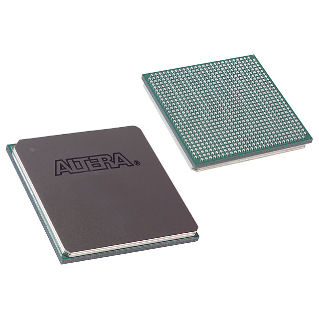
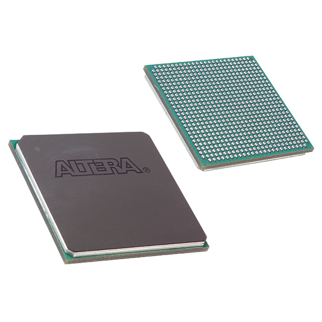
10AX022E3F27I1SG
| Part Description |
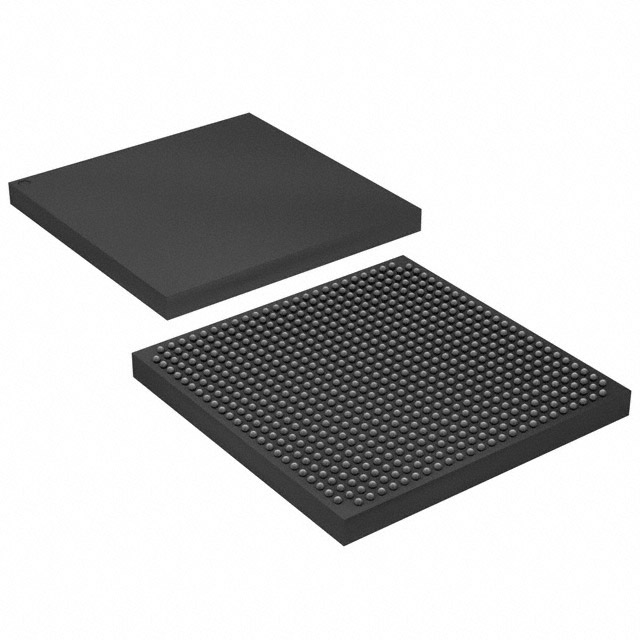
Arria 10 GX Field Programmable Gate Array (FPGA) IC 240 13752320 220000 672-BBGA, FCBGA |
|---|---|
| Quantity | 482 Available (as of June 15, 2026) |

| Product Category | Field Programmable Gate Array (FPGA) |
|---|---|
| Manufacturer | Intel |
| Manufacturing Status | Discontinued |
| Manufacturer Standard Lead Time | 13 Weeks |
| Datasheet |
Specifications & Environmental
| Device Package | 672-FBGA (27x27) | Grade | Industrial | Operating Temperature | -40°C – 100°C | ||
|---|---|---|---|---|---|---|---|
| Package / Case | 672-BBGA, FCBGA | Number of I/O | 240 | Voltage | 870 mV - 930 mV | ||
| Mounting Method | Surface Mount | RoHS Compliance | RoHS Compliant | REACH Compliance | REACH Unaffected | ||
| Moisture Sensitivity Level | 3 (168 Hours) | Number of LABs/CLBs | 80330 | Number of Logic Elements/Cells | 220000 | ||
| Number of Gates | N/A | ECCN | 5A002A1 | HTS Code | 8542.39.0001 | ||
| Qualification | N/A | Total RAM Bits | 13752320 |
Overview of 10AX022E3F27I1SG – Arria 10 GX FPGA, 672‑BBGA (Industrial)
The 10AX022E3F27I1SG is an Intel Arria 10 GX field programmable gate array (FPGA) offered in a 672‑ball BGA FCBGA package for surface-mount applications. It is part of the Arria 10 family of 20 nm mid-range FPGAs, combining a high logic capacity with on‑chip memory and advanced I/O to address midrange, performance‑sensitive designs.
This industrial‑grade device targets markets such as wireless and wireline communications, broadcast, computing and storage, medical imaging, and defense, where a balance of performance, power efficiency and integration is required.
Key Features
- Logic Capacity — 220,000 logic elements provide substantial programmable logic resources for complex digital designs.
- Embedded Memory — 13,752,320 total RAM bits of on‑chip memory for buffering, lookup tables, and data storage within the FPGA fabric.
- I/O and Packaging — 240 user I/Os and a 672‑BBGA (672‑FBGA, 27×27 mm) package designed for surface‑mount assembly.
- Operating Range — Industrial operating temperature range: −40°C to 100°C, suitable for temperature‑demanding deployments.
- Supply Voltage — Core supply specified from 870 mV to 930 mV for core power rail planning.
- High‑Level Architecture — Arria 10 family features referenced in the device overview include Adaptive Logic Modules, variable‑precision DSP blocks, and embedded memory blocks to support mixed compute and signal processing workloads.
- Clocking and PLLs — Integrated clock networks and PLL clock sources are documented for flexible system timing and clock management.
- SerDes and Protocol IP — The Arria 10 overview references low‑power serial transceivers, support for 10 Gbps Ethernet, Interlaken, and PCIe Gen1/Gen2/Gen3 hard IP where applicable within the device family.
- Configuration and Reconfiguration — Series documentation describes support for dynamic and partial reconfiguration and enhanced configuration options for runtime flexibility.
- RoHS Compliant — Device is RoHS compliant for regulatory and assembly compatibility.
Typical Applications
- Wireless Infrastructure — Channel processing and remote radio head applications that require programmable logic and DSP resources to implement baseband and intermediate processing functions.
- Wireline and Networking — Line cards, muxponders and transponder designs leveraging embedded memory, high‑speed serial transceivers, and protocol hard IP for 40G/100G applications.
- Broadcast and Professional AV — Video transport, switching and processing systems that benefit from large logic capacity and on‑chip buffering.
- Compute and Storage Acceleration — Server acceleration, flash cache controllers and cloud compute offload where programmable logic and DSP blocks provide determinism and customization.
- Medical and Defense Systems — Imaging, radar and secure communications systems that require industrial temperature operation and flexible hardware partitioning.
Unique Advantages
- Substantial Logic and Memory in a Single Device: 220,000 logic elements and 13,752,320 RAM bits enable integration of complex control, DSP and buffering functions on one FPGA, reducing external component count.
- Industrial Temperature Range: Rated −40°C to 100°C, supporting deployments in temperature‑challenging environments without derating device selection.
- Compact, Surface‑Mount Packaging: 672‑ball FCBGA (27×27 mm) package provides a high pin count in a board‑friendly surface‑mount form factor for dense designs.
- Rich I/O and Protocol Support: 240 user I/Os combined with series‑level support for PCIe and high‑speed Ethernet protocols simplify integration into networking and compute subsystems.
- Power‑Aware Architecture: Arria 10 family documentation highlights power efficiency techniques and low‑power transceiver options to help manage system power budgets.
Why Choose 10AX022E3F27I1SG?
The 10AX022E3F27I1SG brings the Arria 10 family’s combination of programmable logic, dense embedded memory and advanced I/O to industrial applications that need a balance of performance, integration and environmental robustness. Its specified logic capacity, on‑chip RAM and large I/O count make it suitable for midrange designs that consolidate multiple functions into a single FPGA.
For teams building wireless infrastructure, high‑speed networking, broadcast, compute acceleration or sensor and imaging systems, this industrial‑grade Arria 10 GX device offers a path to reduce BOM complexity while leveraging the documented architecture features of the Arria 10 family.
Request a quote or submit an inquiry to receive pricing, lead‑time and availability information for 10AX022E3F27I1SG.


Date Founded: 1968
Headquarters: Santa Clara, California, USA
Employees: 130,000+
Revenue: $54.23 Billion
Certifications and Memberships: ISO9001:2015, ISO14001:2015, ISO17025:2017, ISO27001:2022, ISO45001:2018, ISO50001:2018


