
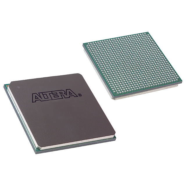
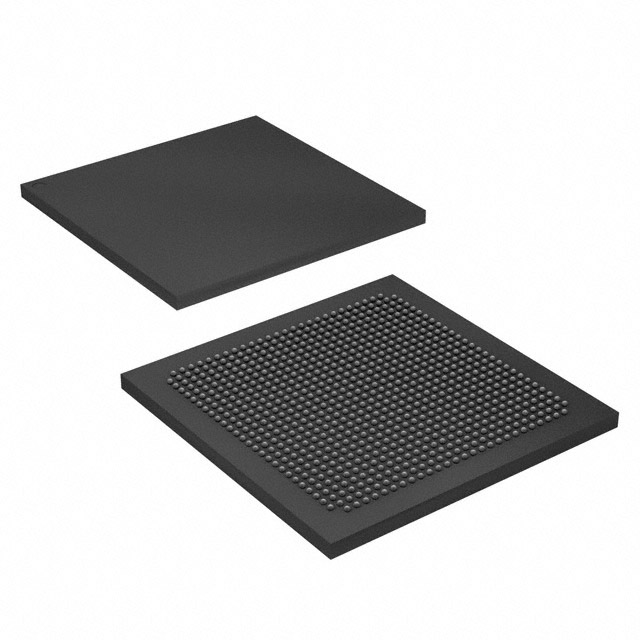
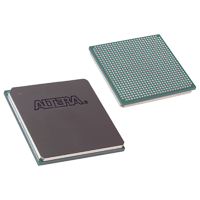
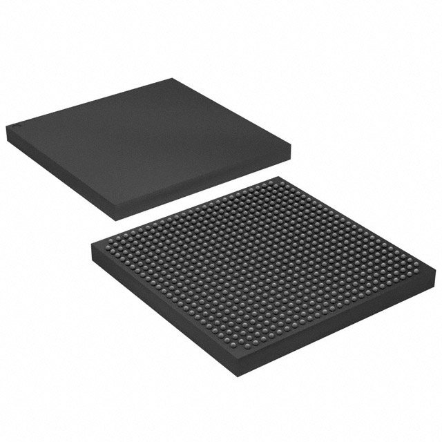
10AX022E3F29E1SG
| Part Description |
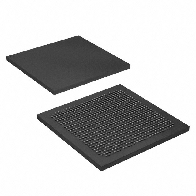
Arria 10 GX Field Programmable Gate Array (FPGA) IC 288 13752320 220000 780-BBGA, FCBGA |
|---|---|
| Quantity | 1,338 Available (as of October 7, 2026) |
| Product Category | Field Programmable Gate Array (FPGA) |
|---|---|
| Manufacturer | Intel |
| Manufacturing Status | Discontinued |
| Manufacturer Standard Lead Time | 13 Weeks |
| Datasheet |
Specifications & Environmental
| Device Package | 780-FBGA (29x29) | Grade | Extended | Operating Temperature | 0°C – 100°C | ||
|---|---|---|---|---|---|---|---|
| Package / Case | 780-BBGA, FCBGA | Number of I/O | 288 | Voltage | 870 mV - 930 mV | ||
| Mounting Method | Surface Mount | RoHS Compliance | RoHS Compliant | REACH Compliance | REACH Unaffected | ||
| Moisture Sensitivity Level | 3 (168 Hours) | Number of LABs/CLBs | 80330 | Number of Logic Elements/Cells | 220000 | ||
| Number of Gates | N/A | ECCN | 5A002A1 | HTS Code | 8542.39.0001 | ||
| Qualification | N/A | Total RAM Bits | 13752320 |
Overview of 10AX022E3F29E1SG – Arria 10 GX FPGA, 220,000 logic elements, 780-FBGA (29×29)
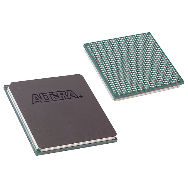
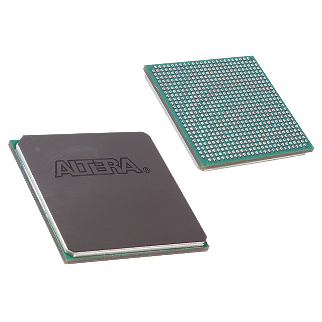
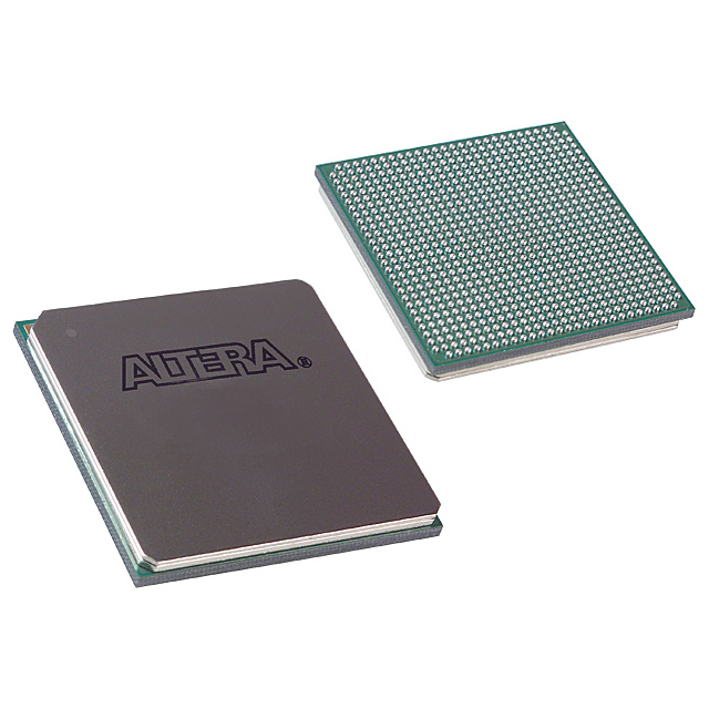
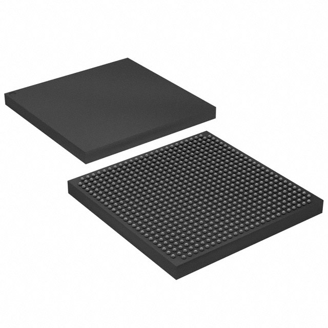
The 10AX022E3F29E1SG is an Intel Arria 10 GX field programmable gate array (FPGA) in a 780-ball FCBGA package. It combines a high logic capacity with embedded memory and programmable I/O to address midrange, performance-sensitive applications.
As a member of the Arria 10 device family, this GX variant targets markets such as wireless, wireline, broadcast, computing and storage, medical, and military applications, delivering performance and power-efficiency characteristics called out by the Arria 10 family documentation.
Key Features
- Logic Capacity — 220,000 logic elements for implementing complex digital functions and custom datapaths.
- Embedded Memory — 13,752,320 total RAM bits to support on-chip buffering, packet storage, or algorithm working memory.
- I/O and Packaging — 288 device I/Os in a 780-BBGA / FCBGA package with supplier package 780-FBGA (29×29); surface-mount mounting type.
- Power Supply — Core voltage supply range of 870 mV to 930 mV for the device core.
- Operating Range and Grade — Extended grade with an operating temperature range of 0 °C to 100 °C.
- Family-Level Capabilities — Arria 10 family features from the datasheet include variable-precision DSP blocks, embedded memory blocks, clock networks with PLL sources, PCIe Gen1/2/3 hard IP, and low-power serial transceivers as architectural capabilities of the device family.
- Compliance — RoHS compliant.
Typical Applications
- Wireless Infrastructure — Channel processing and aggregation functions in remote radio heads and mobile backhaul leveraging high logic density and on-chip memory.
- High‑Speed Wireline — Line cards and mux/ponder modules where programmable logic and family-level PCIe and serial transceiver features support high-throughput packet processing.
- Broadcast and Media — Video switching, transport, and professional audio/video processing using abundant logic and embedded RAM for frame buffering and stream handling.
- Compute and Storage Acceleration — Cloud and server acceleration, flash cache, and server offload tasks that benefit from the device’s DSP and memory resources.
Unique Advantages
- High on‑chip integration: 220,000 logic elements combined with 13.75 Mbits of RAM reduce reliance on external components for many midrange designs.
- Flexible I/O and package options: 288 I/Os in a 780-ball FCBGA (29×29) footprint support a range of board-level interfaces and routing density.
- Power-aware design: The Arria 10 family documentation highlights power-saving technologies; the device’s specified core voltage range supports modern power architectures.
- Extended temperature grade: Rated for 0 °C to 100 °C operation to match many commercial and industrial deployment environments.
- Documented platform: Part of the Intel Arria 10 family with published device overview material, handbook references, and errata documents to aid design and qualification efforts.
Why Choose 10AX022E3F29E1SG?
The 10AX022E3F29E1SG Arria 10 GX FPGA positions itself for midrange designs that require a balance of logic capacity, embedded memory, and family-level I/O and transceiver capabilities. Its 220,000 logic elements and 13.75 Mbits of RAM make it suitable for packet processing, signal processing, and acceleration tasks where on-chip resources reduce system complexity.
Engineers selecting this device gain access to Arria 10 family documentation and architectural features such as DSP blocks, PLL-driven clock networks, and hard IP options, providing a scalable platform for diverse markets including wireless, wireline, broadcast, compute, and medical applications.
Request a quote or submit an inquiry to receive pricing and lead-time information for part number 10AX022E3F29E1SG.





















Date Founded: 1968
Headquarters: Santa Clara, California, USA
Employees: 130,000+
Revenue: $54.23 Billion
Certifications and Memberships: ISO9001:2015, ISO14001:2015, ISO17025:2017, ISO27001:2022, ISO45001:2018, ISO50001:2018


