
10AX022C4U19E3SG
| Part Description |
Arria 10 GX Field Programmable Gate Array (FPGA) IC 240 13752320 220000 484-FBGA |
|---|---|
| Quantity | 324 Available (as of June 15, 2026) |

| Product Category | Field Programmable Gate Array (FPGA) |
|---|---|
| Manufacturer | Intel |
| Manufacturing Status | Active |
| Manufacturer Standard Lead Time | 12 Weeks |
| Datasheet |
Specifications & Environmental
| Device Package | 484-UBGA (19x19) | Grade | Extended | Operating Temperature | 0°C – 100°C | ||
|---|---|---|---|---|---|---|---|
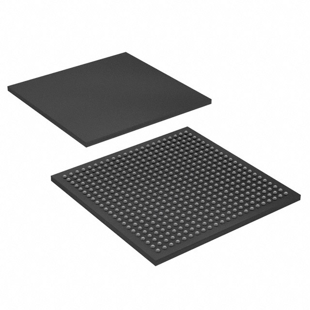
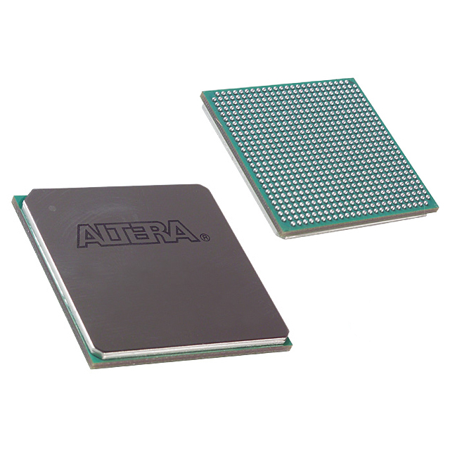
| Package / Case | 484-FBGA | Number of I/O | 240 | Voltage | 870 mV - 980 mV | ||
| Mounting Method | Surface Mount | RoHS Compliance | RoHS Compliant | REACH Compliance | REACH Unaffected | ||
| Moisture Sensitivity Level | 3 (168 Hours) | Number of LABs/CLBs | 80330 | Number of Logic Elements/Cells | 220000 | ||
| Number of Gates | N/A | ECCN | 3A991D | HTS Code | 8542.39.0001 | ||
| Qualification | N/A | Total RAM Bits | 13752320 |
Overview of 10AX022C4U19E3SG – Arria 10 GX FPGA, 220,000 Logic Elements, 484‑FBGA
The 10AX022C4U19E3SG is an Intel Arria 10 GX field-programmable gate array (FPGA) in a 484‑FBGA package. It is part of the Arria 10 device family of 20‑nm mid‑range FPGAs designed for performance and power‑efficiency in a wide range of embedded and networking applications.
This device integrates 220,000 logic elements, 13,752,320 bits of on‑chip RAM and 240 I/O pins, delivering a balanced platform for packet processing, high‑speed interfaces, embedded memory-intensive logic and mid‑range acceleration tasks.
Key Features
- Logic Capacity — 220,000 logic elements suitable for complex mid‑range designs and large FPGA fabric implementations.
- On‑Chip Memory — 13,752,320 total RAM bits for embedded buffers, caches and state storage within the FPGA fabric.
- I/O Density — 240 general‑purpose I/O pins to support multiple parallel interfaces and board‑level connectivity.
- Package & Mounting — 484‑FBGA package (supplier package: 484‑UBGA, 19×19) with surface‑mount mounting for compact board integration.
- Supply Voltage — Core voltage range of 870 mV–980 mV, enabling operation within the specified low‑voltage envelope.
- Operating Range & Grade — Extended grade device with an operating temperature range of 0°C to 100°C.
- Adaptive Logic & DSP — Family features include adaptive logic modules and variable‑precision DSP blocks for arithmetic and signal processing tasks.
- Embedded Memory & External Interfaces — Support for multiple embedded memory types and external memory interfaces appropriate for high‑bandwidth designs.
- Clocking & PLLs — Rich clock network options including PLL clock sources and fractional synthesis for flexible timing architectures.
- High‑Speed SerDes and Protocol IP — Family documentation references low‑power serial transceivers and hard IP for PCIe Gen1/Gen2/Gen3, 10 Gbps Ethernet and Interlaken (as part of Arria 10 features).
- Configuration & Reliability — Supports dynamic and partial reconfiguration, SEU detection and correction and power management capabilities described for Arria 10 devices.
Typical Applications
- Wireless Infrastructure — Channel and switch cards, remote radio head aggregation and mobile backhaul designs that require mid‑range FPGA processing and memory.
- Wireline Networking — Line cards, muxponders/transponders and aggregation modules where programmable logic, embedded memory and high‑speed serial links are required.
- Broadcast & Pro AV — Studio switches, transport and professional audio/video processing leveraging on‑chip memory and DSP capabilities.
- Computing & Storage — Server acceleration, flash cache and cloud compute functions that benefit from programmable logic and integrated memory resources.
- Medical & Defense Systems — Diagnostic imaging, radar and control systems that use configurable logic and embedded resources for specialized processing tasks.
Unique Advantages
- Substantial Logic Fabric: 220,000 logic elements provide the capacity to implement complex algorithms and multi‑function designs on a single device.
- Large On‑Chip RAM: 13.75 Mbit of embedded RAM enables local buffering and data‑flow acceleration without immediate reliance on external memory.
- Balanced I/O & Packaging: 240 I/O pins in a 484‑FBGA (19×19 UBGA) package offer a compact footprint with ample board‑level connectivity.
- Family‑level High‑Speed Support: Arria 10 family features such as serial transceivers and PCIe/10GbE/Interlaken hard IP accelerate implementation of industry protocols.
- Reconfiguration & Reliability: Support for dynamic and partial reconfiguration plus SEU detection/correction options helps maintain uptime and adapt to evolving system needs.
- Extended‑Grade Operation: 0°C to 100°C operating range and extended grade classification for applications requiring wider-than-commercial thermal performance.
Why Choose 10AX022C4U19E3SG?
The 10AX022C4U19E3SG Arria 10 GX FPGA combines sizeable logic capacity, multi‑megabit on‑chip RAM and a high I/O count in a compact 484‑FBGA package, making it suitable for mid‑range systems that demand programmable performance and flexible I/O. Its family‑level features—clocking options, DSP blocks, serial transceivers and protocol hard IP—support data‑intensive tasks common in networking, broadcast and compute acceleration applications.
Designed for engineers who need reconfigurable hardware with a strong balance of performance and power efficiency, this device fits designs that benefit from partial reconfiguration, robust clocking, and embedded memory. The Arria 10 platform also includes documented development flow and device features to support hardware and software development activities.
Request a quote or submit your design inquiry to receive pricing and availability for the 10AX022C4U19E3SG Arria 10 GX FPGA.


Date Founded: 1968
Headquarters: Santa Clara, California, USA
Employees: 130,000+
Revenue: $54.23 Billion
Certifications and Memberships: ISO9001:2015, ISO14001:2015, ISO17025:2017, ISO27001:2022, ISO45001:2018, ISO50001:2018


