
10AX027H3F34E2LG
| Part Description |
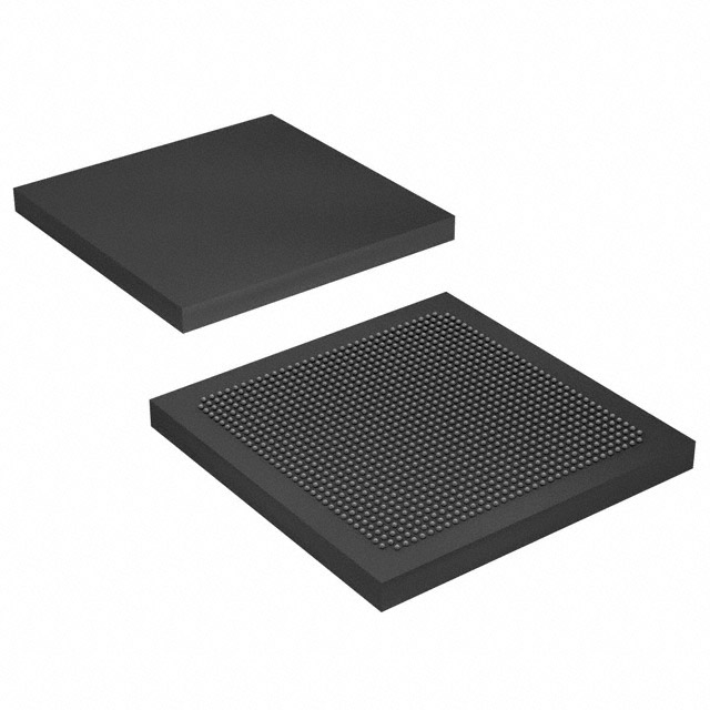
Arria 10 GX Field Programmable Gate Array (FPGA) IC 384 17870848 270000 1152-BBGA, FCBGA |
|---|---|
| Quantity | 299 Available (as of June 15, 2026) |

| Product Category | Field Programmable Gate Array (FPGA) |
|---|---|
| Manufacturer | Intel |
| Manufacturing Status | Active |
| Manufacturer Standard Lead Time | 16 Weeks |
| Datasheet |
Specifications & Environmental
| Device Package | 1152-FBGA, FC (35x35) | Grade | Extended | Operating Temperature | 0°C – 100°C | ||
|---|---|---|---|---|---|---|---|
| Package / Case | 1152-BBGA, FCBGA | Number of I/O | 384 | Voltage | 870 mV - 930 mV | ||
| Mounting Method | Surface Mount | RoHS Compliance | RoHS Compliant | REACH Compliance | REACH Unaffected | ||
| Moisture Sensitivity Level | 3 (168 Hours) | Number of LABs/CLBs | 101620 | Number of Logic Elements/Cells | 270000 | ||
| Number of Gates | N/A | ECCN | 5A002A1 | HTS Code | 8542.39.0001 | ||
| Qualification | N/A | Total RAM Bits | 17870848 |
Overview of 10AX027H3F34E2LG – Arria 10 GX FPGA, 270,000 logic elements, 17,870,848 RAM bits, 384 I/O
The 10AX027H3F34E2LG is an Intel Arria 10 GX field programmable gate array (FPGA) in a 1152-BBGA (FCBGA) package. It implements a mid-range 20 nm FPGA architecture designed for applications that require a balance of performance and power efficiency.
Typical markets for this device include wireless and wireline communications, broadcast, computing and storage, medical imaging, and defense systems. The device combines a high logic element count, substantial embedded memory, and a dense I/O complement to address complex system-level integration needs.
Key Features
- Core Logic 270,000 logic elements provide programmable fabric for complex digital designs and custom logic implementation.
- Embedded Memory 17,870,848 total RAM bits of on-chip memory to support buffering, packet processing, and algorithm acceleration.
- I/O Capacity 384 general-purpose I/O pins for broad interfacing options with external devices, high-pin-count peripherals, and memory interfaces.
- Package & Mounting 1152-BBGA (FCBGA) surface-mount package, supplier package listed as 1152-FBGA FC (35×35), enabling compact board-level integration.
- Power Supply Supported voltage supply range of 870 mV to 930 mV, permitting designs that target the device’s specified core operating window.
- Operating Range & Grade Extended-grade device with an operating temperature range of 0 °C to 100 °C for deployment in a wide set of commercial and industrial-adjacent environments.
- Standards & Family Capabilities Part of the Intel Arria 10 family, which includes device features such as power-saving technologies, fractional synthesis and I/O PLLs, PCIe hard IP, and support for high-speed serial protocols as described in the device overview.
- Compliance RoHS-compliant device supporting modern environmental requirements for lead-free manufacturing.
Typical Applications
- Wireless Infrastructure Channel and switch cards, and mobile backhaul equipment where programmable logic and embedded memory are used for real-time signal processing and protocol offloading.
- Wireline Communications 40G/100G muxponders, transponders, and line cards that benefit from the device’s logic density and I/O capacity for packet processing and line-rate data paths.
- Broadcast & Media Studio switches, video transport, and conferencing equipment that require deterministic processing and high-throughput buffering.
- Computing & Storage Flash cache acceleration and server offload applications leveraging on-chip memory and programmable logic for custom acceleration functions.
- Medical & Defense Systems Diagnostic imaging, radar, and electronic warfare subsystems that use the device’s logic resources and system-level features for signal conditioning and control.
Unique Advantages
- High logic density: 270,000 logic elements enable complex algorithms and large-scale custom logic integration on a single device, reducing board-level component count.
- Substantial on‑chip RAM: 17,870,848 bits of embedded memory support large buffers, lookup tables, and state storage for high-throughput designs.
- Broad I/O connectivity: 384 I/O pins provide flexibility for interfacing to multiple high-speed peripherals and memory devices without extensive external glue logic.
- Compact, manufacturable package: 1152-BBGA (FCBGA) surface-mount package with a 35×35 supplier footprint facilitates dense PCB layouts and automated assembly.
- Designed for power-aware designs: Family-level power-saving technologies and a defined core voltage range (870 mV–930 mV) help manage power in performance-sensitive applications.
- Extended operating range and RoHS compliance: 0 °C to 100 °C operating range and RoHS compliance align with demanding deployment environments and modern manufacturing requirements.
Why Choose 10AX027H3F34E2LG?
The 10AX027H3F34E2LG Arria 10 GX FPGA offers a balanced platform for designers who need significant programmable logic, plentiful embedded memory, and a high I/O count in a compact package. Its specification set supports mid-range, performance-sensitive applications across communications, broadcast, computing, medical, and defense markets.
Backed by Intel’s Arria 10 device documentation and family resources, this device is suitable for engineers seeking a scalable FPGA solution with clear performance and power parameters, supported by established device-level guidance and errata where applicable.
Request a quote or submit a purchasing inquiry to evaluate the 10AX027H3F34E2LG for your next design.


Date Founded: 1968
Headquarters: Santa Clara, California, USA
Employees: 130,000+
Revenue: $54.23 Billion
Certifications and Memberships: ISO9001:2015, ISO14001:2015, ISO17025:2017, ISO27001:2022, ISO45001:2018, ISO50001:2018


