
10AX027H3F34E2SG
| Part Description |
Arria 10 GX Field Programmable Gate Array (FPGA) IC 384 17870848 270000 1152-BBGA, FCBGA |
|---|---|
| Quantity | 1,755 Available (as of June 15, 2026) |

| Product Category | Field Programmable Gate Array (FPGA) |
|---|---|
| Manufacturer | Intel |
| Manufacturing Status | Active |
| Manufacturer Standard Lead Time | 16 Weeks |
| Datasheet |
Specifications & Environmental
| Device Package | 1152-FBGA, FC (35x35) | Grade | Extended | Operating Temperature | 0°C – 100°C | ||
|---|---|---|---|---|---|---|---|
| Package / Case | 1152-BBGA, FCBGA | Number of I/O | 384 | Voltage | 870 mV - 930 mV | ||
| Mounting Method | Surface Mount | RoHS Compliance | RoHS Compliant | REACH Compliance | REACH Unaffected | ||
| Moisture Sensitivity Level | 3 (168 Hours) | Number of LABs/CLBs | 101620 | Number of Logic Elements/Cells | 270000 | ||
| Number of Gates | N/A | ECCN | 5A002A1 | HTS Code | 8542.39.0001 | ||
| Qualification | N/A | Total RAM Bits | 17870848 |
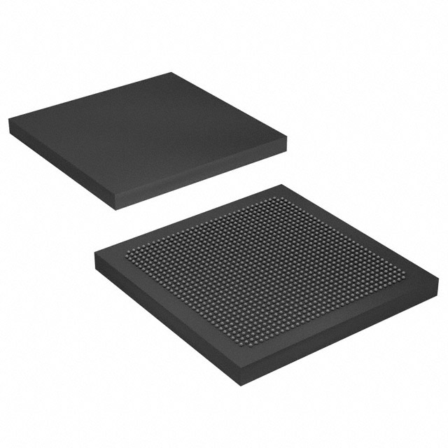
Overview of 10AX027H3F34E2SG – Arria 10 GX FPGA, 270000 logic elements, 1152‑BBGA
The 10AX027H3F34E2SG is an Intel Arria 10 GX family field‑programmable gate array (FPGA) in a 1152‑ball FCBGA surface‑mount package. It combines a large logic capacity with substantial embedded memory and high I/O density, targeting midrange designs that require performance and power efficiency.
Arria 10 devices are positioned for high‑performance, power‑sensitive applications across markets such as wireless, wireline, broadcast, computing and storage, medical, and defense. This device delivers programmable logic, embedded memory, DSP resources and transceiver/IO flexibility suitable for those use cases.
Key Features
- Logic Capacity — 270000 logic elements provide a sizeable programmable fabric for midrange complex designs and system functions.
- Embedded Memory — 17,870,848 total RAM bits of on‑chip memory for buffering, frame storage, and on‑chip data structures.
- I/O Density — 384 general‑purpose I/O pins to support multiple high‑speed interfaces and parallel bus architectures.
- Transceiver & Networking Capabilities — Family documentation lists support for low‑power serial transceivers, Interlaken and 10 Gbps Ethernet features, and enhanced PCS hard IP for high‑speed link implementations.
- DSP and Compute Blocks — Variable‑precision DSP blocks noted in device overview for efficient signal processing and arithmetic workloads.
- Clocking and PLLs — Rich clock network architecture including fractional synthesis and I/O PLLs for flexible clock generation and distribution.
- Configuration & Reconfiguration — Supports dynamic and partial reconfiguration modes as described in the device family overview for flexible in‑field updates.
- Power & Voltage — Core supply range specified at 870 mV to 930 mV to align with the device family’s power management and efficiency features.
- Package & Mounting — 1152‑BBGA (35 × 35) FCBGA surface‑mount package for board‑level integration.
- Operating Range & Grade — Extended temperature grade with specified operating range of 0 °C to 100 °C.
- Compliance — RoHS compliant.
Typical Applications
- Wireless Infrastructure — Channel and switch cards in remote radio heads and mobile backhaul systems where programmable logic and DSP blocks implement channel processing and protocol offload.
- Wireline & Optical Networking — Line cards, muxponders and transponders that require high‑speed serial interfaces and embedded memory for packet buffering and alignment.
- Compute & Storage Acceleration — Server acceleration, flash cache or cloud compute functions that benefit from programmable datapaths, on‑chip RAM and DSP resources.
- Broadcast & Professional AV — Studio switching, video processing and transport applications leveraging the FPGA’s memory and I/O bandwidth for real‑time media handling.
Unique Advantages
- High Logic Density: 270000 logic elements enable complex control, signal processing and protocol implementations without immediate need for external ASICs.
- Substantial On‑Chip Memory: Nearly 17.9 Mb of embedded RAM reduces dependence on external memory for frame buffers and temporary storage.
- Flexible I/O and High‑Speed Links: 384 I/O pins together with family transceiver features allow integration of multiple high‑speed interfaces and parallel buses.
- Power‑Aware Core Voltage: Core supply range of 870 mV–930 mV supports the device family’s power efficiency mechanisms.
- Reconfiguration Capability: Support for dynamic and partial reconfiguration lets designers update or partition logic in the field for evolving requirements.
- Packaged for Production: 1152‑FBGA FCBGA (35 × 35) surface‑mount package provides a compact, production‑ready footprint for board assembly.
Why Choose 10AX027H3F34E2SG?
The 10AX027H3F34E2SG positions itself as a midrange Arria 10 GX FPGA option that balances sizable programmable logic, embedded memory and I/O capacity with the family’s power‑management and clocking features. It is suited to designers who need a programmable platform for signal processing, networking, and system acceleration within a defined operating temperature window.
For projects that require scalable logic, on‑chip RAM, DSP capability and flexible high‑speed I/O in a production FCBGA package, this device offers a combination of integration and capabilities aligned with Arria 10 family design considerations and ecosystem support.
Request a quote or submit a parts inquiry to receive pricing, lead‑time and availability information for the 10AX027H3F34E2SG.


Date Founded: 1968
Headquarters: Santa Clara, California, USA
Employees: 130,000+
Revenue: $54.23 Billion
Certifications and Memberships: ISO9001:2015, ISO14001:2015, ISO17025:2017, ISO27001:2022, ISO45001:2018, ISO50001:2018


