
10AX027H3F35E2SG
| Part Description |
Arria 10 GX Field Programmable Gate Array (FPGA) IC 384 17870848 270000 1152-BBGA, FCBGA |
|---|---|
| Quantity | 123 Available (as of June 15, 2026) |

| Product Category | Field Programmable Gate Array (FPGA) |
|---|---|
| Manufacturer | Intel |
| Manufacturing Status | Active |
| Manufacturer Standard Lead Time | 16 Weeks |
| Datasheet |
Specifications & Environmental
| Device Package | 1152-FBGA, FC (35x35) | Grade | Extended | Operating Temperature | 0°C – 100°C | ||
|---|---|---|---|---|---|---|---|
| Package / Case | 1152-BBGA, FCBGA | Number of I/O | 384 | Voltage | 870 mV - 930 mV | ||
| Mounting Method | Surface Mount | RoHS Compliance | RoHS Compliant | REACH Compliance | REACH Unaffected | ||
| Moisture Sensitivity Level | 3 (168 Hours) | Number of LABs/CLBs | 101620 | Number of Logic Elements/Cells | 270000 | ||
| Number of Gates | N/A | ECCN | 5A002A1 | HTS Code | 8542.39.0001 | ||
| Qualification | N/A | Total RAM Bits | 17870848 |
Overview of 10AX027H3F35E2SG – Arria 10 GX FPGA (270,000 logic elements, 1152-BBGA)
The 10AX027H3F35E2SG is an Intel Arria 10 GX field-programmable gate array (FPGA) IC providing a mid-range, high-performance programmable fabric. Based on the Arria 10 family architecture, this device combines substantial logic capacity with large embedded RAM and a high I/O count for demanding applications in communications, broadcast, computing, medical, and defense markets.
Designed for integration into surface-mount assemblies, the device delivers a balanced set of capabilities for systems that require significant on-chip logic, memory resources, and flexible I/O in a compact 1152-ball BGA package.
Key Features
- Core Logic 270,000 logic elements provide programmable resources for complex signal-processing, control and acceleration tasks.
- Embedded Memory 17,870,848 total RAM bits for on-chip buffering, lookup tables and data storage supporting high-throughput designs.
- I/O 384 I/O pins to interface with external memories, transceivers, and peripheral devices in high-density systems.
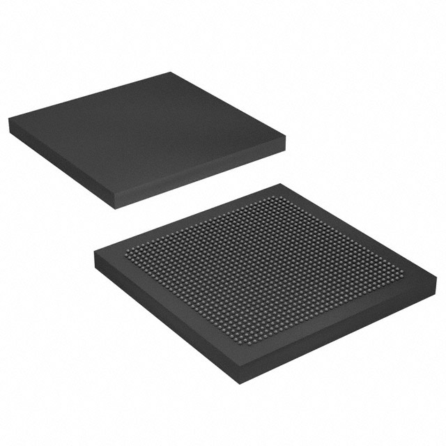
- Package & Mounting 1152-ball BGA (FCBGA) package, supplier device package listed as 1152-FBGA, FC (35×35), optimized for surface-mount PCB assembly.
- Power Supply Core voltage supply range specified from 870 mV to 930 mV to match platform power rails and design margins.
- Operating Range & Grade Extended grade device with an operating temperature range of 0°C to 100°C, suitable for a wide range of commercial and some extended-environment applications.
- Compliance RoHS compliant, meeting common environmental requirements for lead-free assembly.
- Arria 10 Family Capabilities Part of the Intel Arria 10 family (20 nm), which provides architectural features such as advanced clock networks, PLLs, embedded memory blocks, and hard IP blocks referenced in the device overview.
Typical Applications
- Wireless Infrastructure Channel and switch cards, remote radio head subsystems and mobile backhaul designs that require programmable DSP and I/O agility.
- Wireline and Optical Networking Line cards, muxponders and transponders for 40G/100G systems where on-chip logic and memory support packet processing and aggregation.
- Broadcast and Professional AV Studio switches, high-density video processing and transport systems leveraging abundant logic and RAM for real-time media handling.
- Computing and Storage Acceleration Server acceleration, flash cache controllers and cloud compute offload where custom hardware functions and on-chip memory improve throughput.
- Medical and Imaging Diagnostic imaging and scanning systems that need programmable processing blocks and large local memory for image reconstruction tasks.
Unique Advantages
- High logic capacity: 270,000 logic elements allow implementation of large, complex designs on a single FPGA, reducing board-level complexity.
- Significant on-chip memory: Nearly 17.9 Mb of RAM bits supports deep buffering and data-path acceleration without immediate dependence on external memory.
- Flexible I/O integration: 384 I/O pins provide connectivity for high-bandwidth interfaces, peripherals and external memories in compact system layouts.
- Compact, high-pin-count package: 1152-ball FCBGA (35×35) enables dense routing and high pin count in a space-efficient footprint for modern PCBs.
- Extended temperature rating: Grade listed as Extended with 0°C to 100°C operating range for deployment across broader environmental conditions than standard commercial-only parts.
- RoHS compliant and documented platform: Environmentally compliant construction and Arria 10 family documentation support regulatory and design verification needs.
Why Choose 10AX027H3F35E2SG?
The 10AX027H3F35E2SG positions itself as a versatile mid-range FPGA solution that balances large programmable resources, substantial embedded memory and a high I/O count in a single surface-mount FCBGA package. Its specification set is appropriate for system designers building communications, media, compute acceleration and imaging products that demand on-chip logic and memory integration.
Backed by the Arria 10 device family documentation and Intel’s device overview, this part provides an architecture-focused platform for designs that need scalable logic, embedded RAM and configurable I/O while operating within the specified voltage and temperature ranges.
Request a quote or submit an inquiry to receive pricing and availability for the 10AX027H3F35E2SG.


Date Founded: 1968
Headquarters: Santa Clara, California, USA
Employees: 130,000+
Revenue: $54.23 Billion
Certifications and Memberships: ISO9001:2015, ISO14001:2015, ISO17025:2017, ISO27001:2022, ISO45001:2018, ISO50001:2018


