
10AX027H2F35I2LG
| Part Description |
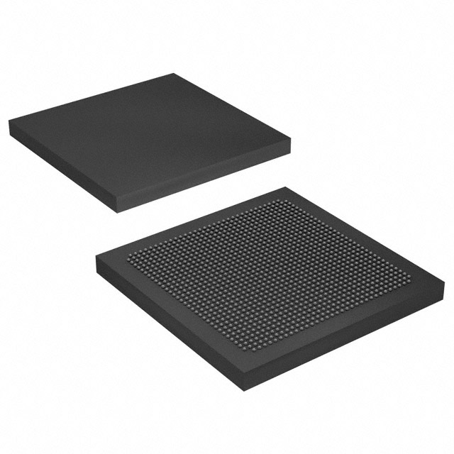
Arria 10 GX Field Programmable Gate Array (FPGA) IC 384 17870848 270000 1152-BBGA, FCBGA |
|---|---|
| Quantity | 538 Available (as of June 10, 2026) |

| Product Category | Field Programmable Gate Array (FPGA) |
|---|---|
| Manufacturer | Intel |
| Manufacturing Status | Active |
| Manufacturer Standard Lead Time | 16 Weeks |
| Datasheet |
Specifications & Environmental
| Device Package | 1152-FBGA, FC (35x35) | Grade | Industrial | Operating Temperature | -40°C – 100°C | ||
|---|---|---|---|---|---|---|---|
| Package / Case | 1152-BBGA, FCBGA | Number of I/O | 384 | Voltage | 870 mV - 980 mV | ||
| Mounting Method | Surface Mount | RoHS Compliance | RoHS Compliant | REACH Compliance | REACH Unaffected | ||
| Moisture Sensitivity Level | 3 (168 Hours) | Number of LABs/CLBs | 101620 | Number of Logic Elements/Cells | 270000 | ||
| Number of Gates | N/A | ECCN | 5A002A1 | HTS Code | 8542.39.0001 | ||
| Qualification | N/A | Total RAM Bits | 17870848 |
Overview of 10AX027H2F35I2LG – Arria 10 GX Field Programmable Gate Array (FPGA) IC
The 10AX027H2F35I2LG is an Intel Arria 10 GX family FPGA offered in a 1152‑ball FCBGA package. It is a 20 nm mid‑range, power‑efficient FPGA architecture designed for performance‑sensitive, midrange applications across wireless, wireline, broadcast, computing and other markets.
With a large logic capacity, extensive embedded memory, and a broad I/O complement, this device targets applications that require high logic density, substantial on‑chip RAM, and industrial temperature operation.
Key Features
- Logic Capacity — 270,000 logic elements to implement complex custom logic, processing pipelines, and protocol stacks.
- On‑chip Memory — 17,870,848 total RAM bits for frame buffering, packet processing, and local data storage.
- I/O Resources — 384 user I/O pins to support broad external interface requirements and dense board-level connectivity.
- Arria 10 GX Family Capabilities — Family features include variable‑precision DSP blocks, embedded memory blocks, clock networks with PLL clock sources, and low‑power serial transceivers as documented for Arria 10 devices.
- High‑speed Interfaces (Family Features) — The Arria 10 device overview documents PCIe Gen1/Gen2/Gen3 hard IP and enhanced PCS hard IP for high‑speed protocols such as 10 Gbps Ethernet and Interlaken.
- Package & Mounting — Surface‑mount 1152‑BBGA (supplier package listed as 1152‑FBGA, FC 35×35) for compact, high‑pin‑count board designs.
- Power & Voltage — Core supply operating range from 870 mV to 980 mV, reflecting the device's low‑voltage core operation.
- Industrial Temperature Range — Rated for operation from −40 °C to 100 °C for deployment in industrial environments.
- RoHS Compliant — Device is RoHS compliant.
Typical Applications
- Wireless Infrastructure — Implement channel and switch cards, remote radio head logic, and mobile backhaul functions using the device's high logic count and embedded RAM for real‑time signal processing and packet handling.
- Wireline and Optical Networking — Build 40G/100G muxponders, transponders and 100G line‑card logic leveraging Arria 10 family high‑speed interface features and substantial on‑chip memory for buffering and protocol processing.
- Compute Acceleration and Storage — Use the large logic element pool and on‑chip RAM for server acceleration, flash cache controllers, and cloud compute offload tasks that require deterministic custom logic.
- Broadcast and Media Processing — Deploy in studio switches, videoconferencing, and professional audio/video equipment where dense logic and plentiful RAM support media processing pipelines.
- Medical and Industrial Systems — Integrate into diagnostic imaging and industrial control applications that benefit from industrial temperature operation and flexible I/O density.
Unique Advantages
- High Logic Density: 270,000 logic elements enable complex algorithms, state machines, and wide datapaths without off‑chip intervention.
- Substantial On‑Chip RAM: 17,870,848 bits of embedded memory reduce external memory dependencies for buffering and local data storage.
- Extensive I/O: 384 I/O pins provide flexible interfacing for multi‑lane protocols, memory interfaces, and mixed signal front‑ends.
- Industrial Temperature Rating: −40 °C to 100 °C supports deployment in industrial and harsh environments.
- Compact High‑Pin Package: 1152‑ball FCBGA (35 × 35 mm supplier package) balances high connectivity with a compact board footprint.
- Arria 10 Family Ecosystem: The device benefits from Arria 10 family features such as variable‑precision DSP blocks, clocking resources, and documented high‑speed interface hard IP for common networking and compute protocols.
Why Choose 10AX027H2F35I2LG?
The 10AX027H2F35I2LG places Arria 10 GX family capabilities into a rugged, industrial‑rated package with a combination of high logic capacity, significant embedded RAM, and a large I/O complement. It is suited to engineers building midrange, performance‑sensitive systems that require on‑chip resources for signal processing, protocol handling, and acceleration tasks.
As part of the Intel Arria 10 device family, this FPGA aligns with documented family features for DSP, transceivers, and high‑speed interface hard IP, offering a scalable route for designs that may evolve across the Arria 10 portfolio while relying on vendor documentation and device handbooks for design guidance.
Request a quote or submit your project requirements to get pricing and availability for the 10AX027H2F35I2LG Arria 10 GX FPGA. Our team can provide lead‑time and configuration support to help integrate this device into your design.


Date Founded: 1968
Headquarters: Santa Clara, California, USA
Employees: 130,000+
Revenue: $54.23 Billion
Certifications and Memberships: ISO9001:2015, ISO14001:2015, ISO17025:2017, ISO27001:2022, ISO45001:2018, ISO50001:2018


