
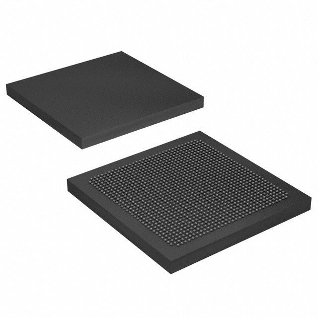
10AX032H2F35E1SG
| Part Description |
Arria 10 GX Field Programmable Gate Array (FPGA) IC 384 21040128 320000 1152-BBGA, FCBGA |
|---|---|
| Quantity | 722 Available (as of June 14, 2026) |
| Product Category | Field Programmable Gate Array (FPGA) |
|---|---|
| Manufacturer | Intel |
| Manufacturing Status | Discontinued |
| Manufacturer Standard Lead Time | 13 Weeks |
| Datasheet |
Specifications & Environmental
| Device Package | 1152-FCBGA (35x35) | Grade | Extended | Operating Temperature | 0°C – 100°C | ||
|---|---|---|---|---|---|---|---|
| Package / Case | 1152-BBGA, FCBGA | Number of I/O | 384 | Voltage | 870 mV - 980 mV | ||
| Mounting Method | Surface Mount | RoHS Compliance | RoHS Compliant | REACH Compliance | REACH Unaffected | ||
| Moisture Sensitivity Level | 3 (168 Hours) | Number of LABs/CLBs | 119900 | Number of Logic Elements/Cells | 320000 | ||
| Number of Gates | N/A | ECCN | 5A002A1 | HTS Code | 8542.39.0001 | ||
| Qualification | N/A | Total RAM Bits | 21040128 |
Overview of 10AX032H2F35E1SG – Arria 10 GX Field Programmable Gate Array (FPGA) IC 384 21040128 320000 1152-BBGA, FCBGA
The 10AX032H2F35E1SG is an Intel Arria 10 GX-series FPGA in a 1152-ball FCBGA package designed for mid-range, performance-sensitive applications. It is part of the Arria 10 device family of 20 nm FPGAs and SoCs that deliver higher performance and power efficiency for markets such as wireless, wireline, broadcast, computing and storage, medical, and defense.
Key on-chip resources include 320,000 logic elements, 21,040,128 bits of embedded RAM, and 384 I/O pins, making this device suitable for complex hardware acceleration, high-density I/O interfacing, and memory-rich processing tasks while operating within an extended-grade temperature range.
Key Features
- Core Logic 320,000 logic elements provide a large programmable fabric for implementing complex digital designs and hardware-accelerated functions.
- On-chip Memory 21,040,128 total RAM bits of embedded memory for high-bandwidth buffering, lookup tables, and data storage within the FPGA fabric.
- I/O Capacity 384 user I/O pins support dense external interfacing and connectivity for multi-channel applications and high-pin-count systems.
- Package and Mounting 1152-FCBGA (35 × 35 mm) package in a 1152-BBGA case; designed for surface-mount assembly in compact, high-pin-count designs.
- Power Rail Core voltage supply range specified at 0.870 V to 0.980 V, enabling integration into systems with low-voltage FPGA power domains.
- Operating Range & Grade Extended-grade device with an operating temperature range of 0 °C to 100 °C suitable for many commercial and industrial environments.
- Family-Level Capabilities As part of the Arria 10 family, the device leverages series features such as variable-precision DSP blocks, embedded memory blocks, clocking networks and PLLs, low-power serial transceivers, and available PCIe/10Gb Ethernet hard IP (refer to family documentation for configuration specifics).
- Compliance RoHS compliant for environmental conformity in lead-free manufacturing processes.
Typical Applications
- Wireless Infrastructure Channel processing, switch cards, and remote radio head designs that need programmable logic, DSP resources, and significant on-chip memory.
- High-Speed Networking Line cards, muxponders, and aggregation equipment where dense I/O and programmable protocol handling are required.
- Video & Broadcast Studio switches, video processing, and transport systems that benefit from large logic capacity and embedded RAM for frame buffering and real-time processing.
- Compute Acceleration & Storage Server offload, flash cache controllers, and acceleration tasks that use FPGA-based custom pipelines and memory-rich data paths.
- Medical & Defense Systems Diagnostic imaging, radar, and electronic control systems that require configurable logic, on-chip memory, and extended operating temperature capability.
Unique Advantages
- High Logic Density: 320,000 logic elements enable implementation of large, parallel hardware functions and complex state machines within a single device.
- Substantial Embedded Memory: Over 21 million bits of on-chip RAM reduce external memory dependency for buffering and accelerate in-fabric data processing.
- Robust I/O Footprint: 384 user I/Os support multi-channel interfacing and high-pin-count peripherals without intermediary glue logic.
- Compact High-Pin Package: 1152-FCBGA (35 × 35 mm) packaging provides a balance of pin count and board-space efficiency for dense system designs.
- Low-Voltage Core Support: Narrow core voltage range (0.870–0.980 V) aligns with modern system power domains for efficient power delivery and management.
- Family Ecosystem & Documentation: Being part of the Intel Arria 10 family gives access to device family documentation, design recommendations, and configuration options for transceivers, DSPs, memory interfaces, and PLL/clocking resources.
Why Choose 10AX032H2F35E1SG?
The 10AX032H2F35E1SG Arria 10 GX FPGA combines a large logic fabric, significant on-chip RAM, and a high I/O count in a compact FCBGA package to address mid-range, performance- and memory-intensive designs. Its extended operating grade and RoHS compliance make it suitable for deployments across networking, broadcast, compute acceleration, medical imaging, and defense systems that require a programmable, high-density hardware implementation.
Engineers and procurement teams benefit from the Arria 10 family ecosystem and documentation to streamline integration, power planning, and system-level design validation while leveraging the device’s balance of logic, memory, and I/O resources for scalable hardware solutions.
If you would like pricing, availability, or a formal quote for part number 10AX032H2F35E1SG, submit a request or sales inquiry and include your required quantity and delivery timeframe.


Date Founded: 1968
Headquarters: Santa Clara, California, USA
Employees: 130,000+
Revenue: $54.23 Billion
Certifications and Memberships: ISO9001:2015, ISO14001:2015, ISO17025:2017, ISO27001:2022, ISO45001:2018, ISO50001:2018


