
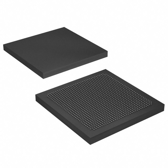
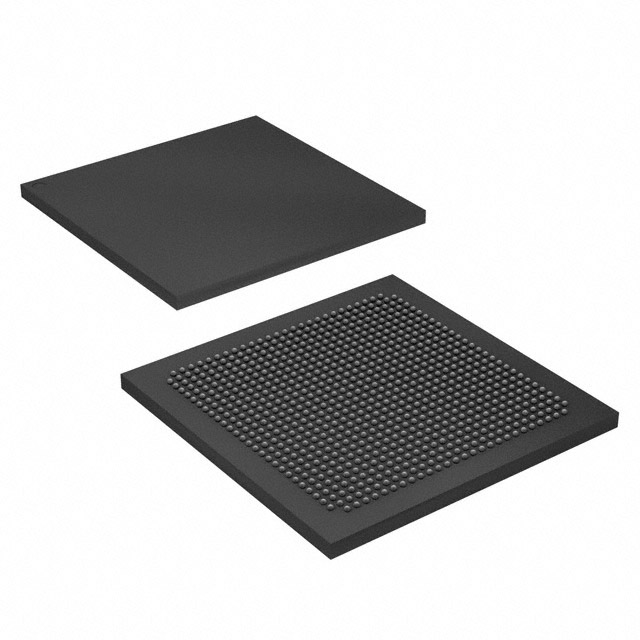
10AX048H1F34E1HG
| Part Description |
Arria 10 GX Field Programmable Gate Array (FPGA) IC 492 5664768 480000 1152-BBGA, FCBGA |
|---|---|
| Quantity | 327 Available (as of June 10, 2026) |

| Product Category | Field Programmable Gate Array (FPGA) |
|---|---|
| Manufacturer | Intel |
| Manufacturing Status | Active |
| Manufacturer Standard Lead Time | 16 Weeks |
| Datasheet |
Specifications & Environmental
| Device Package | 1152-FCBGA (35x35) | Grade | Extended | Operating Temperature | 0°C – 100°C | ||
|---|---|---|---|---|---|---|---|
| Package / Case | 1152-BBGA, FCBGA | Number of I/O | 492 | Voltage | 870 mV - 980 mV | ||
| Mounting Method | Surface Mount | RoHS Compliance | RoHS Compliant | REACH Compliance | REACH Unaffected | ||
| Moisture Sensitivity Level | 3 (168 Hours) | Number of LABs/CLBs | 183590 | Number of Logic Elements/Cells | 480000 | ||
| Number of Gates | N/A | ECCN | 5A002A1 | HTS Code | 8542.39.0001 | ||
| Qualification | N/A | Total RAM Bits | 5664768 |
Overview of 10AX048H1F34E1HG – Arria 10 GX FPGA, 1152-FCBGA
The 10AX048H1F34E1HG is an Intel Arria 10 GX field-programmable gate array (FPGA) in a 1152-FCBGA (35×35) package. As part of the Arria 10 device family, this 20 nm mid-range FPGA targets high-performance, power-sensitive applications across wireless, wireline, broadcast, computing, storage, medical, and defense markets.
This device combines a large logic fabric with embedded memory and on-chip transceiver/clock features to support midrange designs that require high logic density, substantial on-chip RAM, and a flexible I/O count while operating within a low-voltage core supply range.
Key Features
- Logic Capacity — 480,000 logic element cells provide significant programmable logic resources for complex midrange designs.
- Embedded Memory — 5,664,768 total RAM bits of on-chip memory to support buffering, packet processing, and system-level data handling.
- I/O Count — 492 user I/O pins to connect multiple external interfaces and peripherals without sacrificing board-level routing flexibility.
- Transceivers and Interfaces — Arria 10 devices include low-power serial transceivers and hard IP such as PCIe (Gen1/Gen2/Gen3) and enhanced PCS hard IP for Interlaken and 10 Gbps Ethernet (family-level capabilities referenced in device overview).
- DSP and Math Acceleration — Variable-precision DSP blocks are available in the Arria 10 family to accelerate signal processing and compute-intensive kernels.
- Clocking and PLLs — Fractional synthesis and I/O PLLs provide flexible clock generation and distribution for high-performance timing architectures.
- Package & Mounting — Supplier device package: 1152-FCBGA (35×35); package case listed as 1152-BBGA, suitable for surface-mount assembly.
- Power & Operating Range — Core supply range: 870 mV to 980 mV; operating temperature range: 0 °C to 100 °C; device grade: Extended.
- Compliance — RoHS compliant.
Typical Applications
- Wireless Infrastructure — Channel and switch card functions in remote radio heads and mobile backhaul equipment where programmable logic and DSP accelerate baseband and control functions.
- Wireline Networking — 40G/100G muxponders, transponders and line cards that require integrated transceivers and high logic density for packet processing and protocol handling.
- Broadcast & Professional AV — Studio switching, videoconferencing, and professional audio/video processing leveraging on-chip memory and DSP resources.
- Computing & Storage — Flash cache, server acceleration, and cloud computing server offload tasks that benefit from reconfigurable logic and embedded memory.
- Medical & Defense Systems — Diagnostic imaging, radar, and electronic warfare subsystems where programmable performance and on-chip processing are required.
Unique Advantages
- High Logic Density: 480,000 logic element cells enable complex designs and system consolidation onto a single FPGA.
- Substantial On-Chip Memory: 5.66 Mbit of RAM bits reduces dependency on external memory for buffering and local data storage, simplifying board design.
- Rich I/O and Interface Support: 492 I/O pins plus family-level support for PCIe and high-speed Ethernet/Interlaken hard IP streamline connectivity and protocol integration.
- Power-Aware Architecture: Low core-voltage operating range (870–980 mV) supports power-sensitive implementations and helps manage thermal profiles.
- Flexible Clocking and DSP: Integrated PLLs and variable-precision DSP blocks provide deterministic timing and efficient signal-processing acceleration.
- Extended Grade and Compliance: Extended temperature grade (0 °C to 100 °C) and RoHS compliance suit a broad set of application environments and regulatory needs.
Why Choose 10AX048H1F34E1HG?
The 10AX048H1F34E1HG Arria 10 GX FPGA balances high logic capacity, significant embedded RAM, and a broad I/O complement within a compact 1152-FCBGA package. It is well-suited for midrange applications that require programmable acceleration, moderate to high-speed serial interfaces, and power-efficient operation.
Designed as part of the Intel Arria 10 family, this device benefits from a documented device overview and ecosystem support aimed at helping engineers scale designs, manage power, and integrate transceivers and hard IP. Its combination of resources and extended operating grade makes it appropriate for teams developing wireless, wireline, broadcast, computing, medical, or defense systems that need programmable, high-density logic with on-chip memory and interface flexibility.
If you require pricing, availability, or a formal quote for part number 10AX048H1F34E1HG, request a quote or submit an inquiry to our sales team for a fast response.


Date Founded: 1968
Headquarters: Santa Clara, California, USA
Employees: 130,000+
Revenue: $54.23 Billion
Certifications and Memberships: ISO9001:2015, ISO14001:2015, ISO17025:2017, ISO27001:2022, ISO45001:2018, ISO50001:2018


