
10AX090U3F45E2SG
| Part Description |
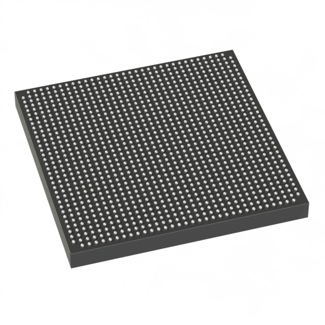
Arria 10 GX Field Programmable Gate Array (FPGA) IC 480 59234304 900000 1932-BBGA, FCBGA |
|---|---|
| Quantity | 1,450 Available (as of June 15, 2026) |

| Product Category | Field Programmable Gate Array (FPGA) |
|---|---|
| Manufacturer | Intel |
| Manufacturing Status | Active |
| Manufacturer Standard Lead Time | 16 Weeks |
| Datasheet |
Specifications & Environmental
| Device Package | 1932-FCBGA (45x45) | Grade | Extended | Operating Temperature | 0°C – 100°C | ||
|---|---|---|---|---|---|---|---|
| Package / Case | 1932-BBGA, FCBGA | Number of I/O | 480 | Voltage | 870 mV - 930 mV | ||
| Mounting Method | Surface Mount | RoHS Compliance | RoHS Compliant | REACH Compliance | REACH Unaffected | ||
| Moisture Sensitivity Level | 3 (168 Hours) | Number of LABs/CLBs | 339620 | Number of Logic Elements/Cells | 900000 | ||
| Number of Gates | N/A | ECCN | 3A001A7A | HTS Code | 8542.39.0001 | ||
| Qualification | N/A | Total RAM Bits | 59234304 |
Overview of 10AX090U3F45E2SG – Arria 10 GX FPGA, 900,000 logic elements, 59,234,304 bits RAM, 480 I/Os
The 10AX090U3F45E2SG is an Intel Arria 10 GX field programmable gate array (FPGA) offered in a 1932-ball FCBGA (45 × 45) package. It delivers a high logic capacity and large embedded RAM in a surface-mount package, suitable for midrange designs that require significant programmable logic and I/O integration.
As part of the Intel Arria 10 family of 20 nm mid-range FPGAs and SoCs, this device combines performance and power-efficiency characteristics intended for applications across communications, broadcast, compute/storage, medical, and defense markets.
Key Features
- Core architecture 20 nm Arria 10 family device architecture noted for mid-range FPGA and SoC class designs; described in manufacturer materials as delivering higher performance and power efficiency within its class.
- Logic capacity 900,000 logic elements provide high programmable logic density for complex custom logic, state machines, and hardware accelerators.
- Embedded memory 59,234,304 total RAM bits supplied as on-chip embedded memory blocks to support large buffering, frame storage, and on-chip data structures.
- I/O 480 device I/Os available to interface with external components and memory, enabling broad system connectivity and high pin-count designs.
- Power and core supply Specified core voltage range of 870 mV to 930 mV for the device core supply to guide power delivery and sequencing on the board.
- Packaging and mounting 1932-ball FCBGA (1932-BBGA) package, 45 × 45 mm supplier device package, designed for surface-mount assembly.
- Operating range and grade Extended grade device with operating temperature range 0 °C to 100 °C.
- Family-level system features Arria 10 family documentation highlights embedded memory blocks, adaptive logic modules, clock networks and PLL clock sources, variable-precision DSP blocks, PCIe Gen1/Gen2/Gen3 hard IP, and low-power serial transceiver support as part of the family feature set.
- Standards and compliance RoHS compliant per supplier data.
Typical Applications
- Wireless infrastructure Channel and switch cards in remote radio heads and mobile backhaul equipment where programmable logic and on-chip memory accelerate signal processing and control.
- Wireline and metro networking 40G/100G muxponders, transponders, and line cards that require substantial logic and I/O capacity for packet processing and bridging functions.
- Broadcast and media Studio switches, professional audio/video transport and processing systems that use embedded RAM and custom logic pipelines for low-latency media handling.
- Compute and storage Flash cache, cloud server acceleration, and storage controllers where on-chip logic and RAM support data-path acceleration and buffering.
- Medical and imaging Diagnostic imaging and scanner systems that use programmable data flows and local memory for acquisition and preprocessing tasks.
Unique Advantages
- High logic density: 900,000 logic elements enable integration of large custom hardware functions and consolidation of multiple logic blocks into a single device.
- Substantial on-chip RAM: 59,234,304 bits of embedded RAM reduce external memory dependence for buffering, frame storage, and real-time data handling.
- Large I/O complement: 480 I/Os simplify board-level integration and provide flexibility for parallel interfaces and multiple memory or peripheral connections.
- Compact, assembly-ready package: 1932-ball FCBGA (45 × 45) surface-mount package supports high-density PCB designs and automated assembly flows.
- Designed for power-managed designs: Specified core voltage range (870 mV–930 mV) supports tightly controlled power-delivery design and system-level power management.
- Extended temperature grade: Rated 0 °C to 100 °C to match equipment environments that require wider-than-commercial thermal operating range.
Why Choose 10AX090U3F45E2SG?
The 10AX090U3F45E2SG positions itself as a high-capacity Arria 10 GX FPGA option for mid-range systems where a combination of large programmable logic, significant embedded RAM, and a broad I/O count are required. Its packaging, power specifications, and extended temperature grade make it suitable for complex board-level designs that demand integration and deterministic on-chip resources.
As part of the Intel Arria 10 family, this device benefits from the family’s documented design features—such as advanced clocking, DSP capabilities, embedded memory architectures, and supported protocol hard IP—helping teams scale designs across similar device classes and leverage available documentation and design flows.
Request a quote or submit a pricing inquiry to receive availability and lead-time details for the 10AX090U3F45E2SG and to discuss how it fits into your next design.


Date Founded: 1968
Headquarters: Santa Clara, California, USA
Employees: 130,000+
Revenue: $54.23 Billion
Certifications and Memberships: ISO9001:2015, ISO14001:2015, ISO17025:2017, ISO27001:2022, ISO45001:2018, ISO50001:2018


