
10AX090U4F45E3LG
| Part Description |
Arria 10 GX Field Programmable Gate Array (FPGA) IC 480 59234304 900000 1932-BBGA, FCBGA |
|---|---|
| Quantity | 1,755 Available (as of June 15, 2026) |

| Product Category | Field Programmable Gate Array (FPGA) |
|---|---|
| Manufacturer | Intel |
| Manufacturing Status | Active |
| Manufacturer Standard Lead Time | 16 Weeks |
| Datasheet |
Specifications & Environmental
| Device Package | 1932-FCBGA (45x45) | Grade | Extended | Operating Temperature | 0°C – 100°C | ||
|---|---|---|---|---|---|---|---|
| Package / Case | 1932-BBGA, FCBGA | Number of I/O | 480 | Voltage | 870 mV - 930 mV | ||
| Mounting Method | Surface Mount | RoHS Compliance | RoHS Compliant | REACH Compliance | REACH Unaffected | ||
| Moisture Sensitivity Level | 3 (168 Hours) | Number of LABs/CLBs | 339620 | Number of Logic Elements/Cells | 900000 | ||
| Number of Gates | N/A | ECCN | 3A001A7A | HTS Code | 8542.39.0001 | ||
| Qualification | N/A | Total RAM Bits | 59234304 |
Overview of 10AX090U4F45E3LG – Arria 10 GX FPGA, 900,000 Logic Elements, 1932-FCBGA
The 10AX090U4F45E3LG is an Intel Arria 10 GX field programmable gate array (FPGA) delivered in a 1932-FCBGA (45×45) package. As part of the Arria 10 family of 20 nm mid-range FPGAs and SoCs, this device targets high‑performance, power‑sensitive applications across wireless, wireline, broadcast, computing and storage, medical, and defense markets.
With 900,000 logic elements, substantial embedded memory, and broad I/O capability, the device is built to handle complex data-paths, high‑speed interfaces, and memory‑intensive processing in constrained board-space and thermal envelopes.
Key Features
- Logic Capacity — 900,000 logic elements (logic element cells) provide dense programmable logic for large, complex designs and high‑level integration.
- On‑Chip Memory — 59,234,304 total RAM bits of embedded memory to support buffering, caches, and data‑flow storage directly on the FPGA fabric.
- I/O and Interfaces — Up to 480 I/O pins for broad external connectivity and system interfacing.
- High‑Speed Serial and Protocol Support (family) — Arria 10 devices include low‑power serial transceivers and hard IP for protocols such as PCIe Gen1/2/3, 10 Gbps Ethernet, and Interlaken as documented for the device family.
- DSP and Timing Resources (family) — The Arria 10 family provides variable‑precision DSP blocks and advanced clock networks with PLLs to support high-performance signal processing and timing flexibility.
- Power Supply and Management — Rated supply voltage range of 870 mV to 930 mV, enabling fine‑grained power management and voltage planning for system designs.
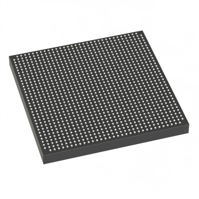
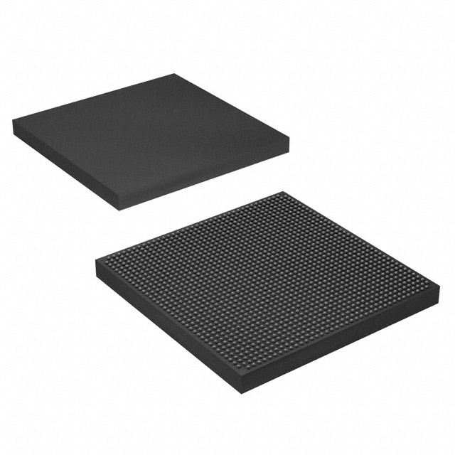
- Package and Mounting — 1932‑ball FCBGA (45×45) surface‑mount package for compact board integration.
- Operating Range and Grade — Extended‑grade device with an operating temperature range of 0 °C to 100 °C and RoHS compliance for environmental requirements.
Typical Applications
- Wireless Infrastructure — Implements channel processing, switching and mobile backhaul functions that benefit from dense logic and on‑chip memory for packet buffering and real‑time signal processing.
- Wireline and Optical Networking — Suits 40G/100G muxponder and line‑card designs where high logic capacity, embedded memory, and serial transceiver support (family) enable protocol handling and packet aggregation.
- Data Center Acceleration — Ideal for server acceleration, flash cache controllers and cloud compute offload tasks that require large programmable resources and extensive I/O.
- Broadcast and Professional AV — Enables studio switching, video processing and transport functions using abundant logic and memory resources for real‑time media handling.
Unique Advantages
- High Logic Density: 900,000 logic elements enable consolidation of multiple functions into a single FPGA, reducing board‑level component count.
- Substantial Embedded Memory: 59,234,304 RAM bits support large frame buffers, caches and streaming pipelines without immediate dependence on external memory.
- Extensive I/O: 480 I/O pins provide flexibility for diverse peripheral interfaces and multi‑board interconnects.
- Family‑Level High‑Speed Interfaces: Arria 10 family documentation describes built‑in support for PCIe Gen1/2/3, 10 Gbps Ethernet, and Interlaken hard IP, simplifying implementation of standard communication links.
- Compact, High‑Pin Package: 1932‑ball FCBGA (45×45) package enables dense routing and small PCB footprint for space‑constrained systems.
- Extended‑Grade and RoHS Compliant: Rated 0 °C to 100 °C and RoHS compliant for designs requiring extended operating range and environmental compliance.
Why Choose 10AX090U4F45E3LG?
The 10AX090U4F45E3LG Arria 10 GX FPGA combines high logic capacity, large on‑chip memory, and broad I/O to address demanding mid‑range applications that require both performance and energy‑aware design. Its placement in the Arria 10 family means designers can leverage family‑level features—such as advanced DSP resources, clocking infrastructure, and hard IP for common high‑speed protocols—while aligning supply and thermal budgets through a defined core voltage range.
This device is suitable for engineering teams building network equipment, compute accelerators, broadcast systems, and other applications that need scalable programmable logic, robust memory resources, and compact packaging backed by Intel’s Arria 10 documentation and ecosystem.
Request a quote or submit a pricing inquiry for 10AX090U4F45E3LG to check availability and delivery for your next design.


Date Founded: 1968
Headquarters: Santa Clara, California, USA
Employees: 130,000+
Revenue: $54.23 Billion
Certifications and Memberships: ISO9001:2015, ISO14001:2015, ISO17025:2017, ISO27001:2022, ISO45001:2018, ISO50001:2018


