
10AX115N3F45I2SG
| Part Description |
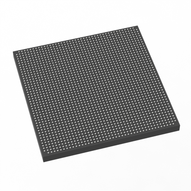
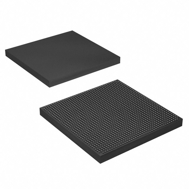
Arria 10 GX Field Programmable Gate Array (FPGA) IC 768 68857856 1150000 1932-BBGA, FCBGA |
|---|---|
| Quantity | 1,171 Available (as of June 9, 2026) |

| Product Category | Field Programmable Gate Array (FPGA) |
|---|---|
| Manufacturer | Intel |
| Manufacturing Status | Active |
| Manufacturer Standard Lead Time | 16 Weeks |
| Datasheet |
Specifications & Environmental
| Device Package | 1932-FCBGA (45x45) | Grade | Industrial | Operating Temperature | -40°C – 100°C | ||
|---|---|---|---|---|---|---|---|
| Package / Case | 1932-BBGA, FCBGA | Number of I/O | 768 | Voltage | 870 mV - 930 mV | ||
| Mounting Method | Surface Mount | RoHS Compliance | RoHS Compliant | REACH Compliance | REACH Unaffected | ||
| Moisture Sensitivity Level | 3 (168 Hours) | Number of LABs/CLBs | 427200 | Number of Logic Elements/Cells | 1150000 | ||
| Number of Gates | N/A | ECCN | 3A001A7A | HTS Code | 8542.39.0001 | ||
| Qualification | N/A | Total RAM Bits | 68857856 |
Overview of 10AX115N3F45I2SG – Arria 10 GX FPGA, 1,150,000 logic elements, 1932-FCBGA
The 10AX115N3F45I2SG is an Intel Arria 10 GX field programmable gate array (FPGA) IC built on the Arria 10 device family architecture. It combines high logic density and substantial on-chip memory with features from the Arria 10 series to address mid-range, performance- and power-sensitive applications.
Designed for markets such as wireless, wireline, broadcast, computing and storage, medical, and defense, this device targets applications that require extensive I/O, large embedded RAM, and scalable logic capacity while operating across an industrial temperature range.
Key Features
- 20 nm Arria 10 Architecture The device leverages the Arria 10 family architecture for mid-range, high-performance, power-efficient FPGA designs as described in the device overview.
- High Logic Capacity Provides 1,150,000 logic elements (cells) and 427,200 adaptive logic modules as platform building blocks for complex logic integration.
- Large Embedded Memory 68,857,856 total RAM bits of on-chip memory to support buffering, caching, and high-throughput data processing.
- Extensive I/O Up to 768 I/O pins to support broad external connectivity and multiple parallel interfaces.
- Signal Processing and SerDes Series-level features include variable-precision DSP blocks and low-power serial transceivers for high-speed data and signal-processing tasks, as described in the Arria 10 device overview.
- Power and Clocking Support for advanced clock networks, fractional synthesis and I/O PLLs; specified supply voltage range is 870 mV to 930 mV to meet core power requirements.
- Package and Mounting Available in a 1932-BBGA / 1932-FCBGA supply package (1932-FCBGA (45×45)) and intended for surface-mount assembly.
- Industrial Temperature Range Rated to operate from -40 °C to 100 °C for deployment in industrial environments.
- Regulatory RoHS compliant.
Typical Applications
- Wireless Infrastructure Channel and switch cards in remote radio heads and mobile backhaul systems that require dense logic and high memory bandwidth.
- Wireline and Optical Networking 40G/100G muxponders, transponders, and 100G line cards where high-speed serial interfaces and large on-chip memory are required.
- Broadcast and Media Processing Studio switches, videoconferencing, and professional audio/video processing that benefit from large logic capacity and embedded RAM.
- Computing and Storage Acceleration Flash cache, cloud server acceleration, and storage controllers leveraging dense logic and DSP resources for data-path acceleration.
Unique Advantages
- High-density logic integration: 1,150,000 logic elements enable consolidation of complex functions into a single device, reducing board-level component count.
- Significant on-chip memory: 68,857,856 RAM bits provide ample capacity for buffering and packet or frame storage without immediate external memory dependence.
- Broad external connectivity: 768 I/O pins allow flexible interfacing to multiple peripherals, memory devices, and high-speed links.
- Industrial-ready thermal range: Rated for -40 °C to 100 °C operation to suit demanding environmental deployments.
- Compact, surface-mount FCBGA package: The 1932-FCBGA (45×45) package offers a high pin-count, compact solution for space-constrained boards.
- Low-voltage core operation: Specified supply range of 870 mV to 930 mV supports modern low-voltage power infrastructures.
Why Choose 10AX115N3F45I2SG?
The 10AX115N3F45I2SG places Arria 10 GX series capabilities—high logic density, substantial embedded memory, extensive I/O, and series-level DSP and transceiver features—into a single industrial-temperature FCBGA package. It is positioned for designers who need a balance of performance and power efficiency for mid-range applications across networking, communications, broadcast, compute acceleration, and industrial systems.
With a combination of large on-chip resources, flexible clocking and power options, and RoHS compliance, this device offers a scalable platform for integrating complex digital functions while keeping board-level complexity manageable and supporting long-term design needs.
Request a quote or submit an inquiry for part number 10AX115N3F45I2SG to receive pricing and availability information and to discuss how this FPGA can meet your project requirements.


Date Founded: 1968
Headquarters: Santa Clara, California, USA
Employees: 130,000+
Revenue: $54.23 Billion
Certifications and Memberships: ISO9001:2015, ISO14001:2015, ISO17025:2017, ISO27001:2022, ISO45001:2018, ISO50001:2018


