
10AX115S3F45E2LG
| Part Description |
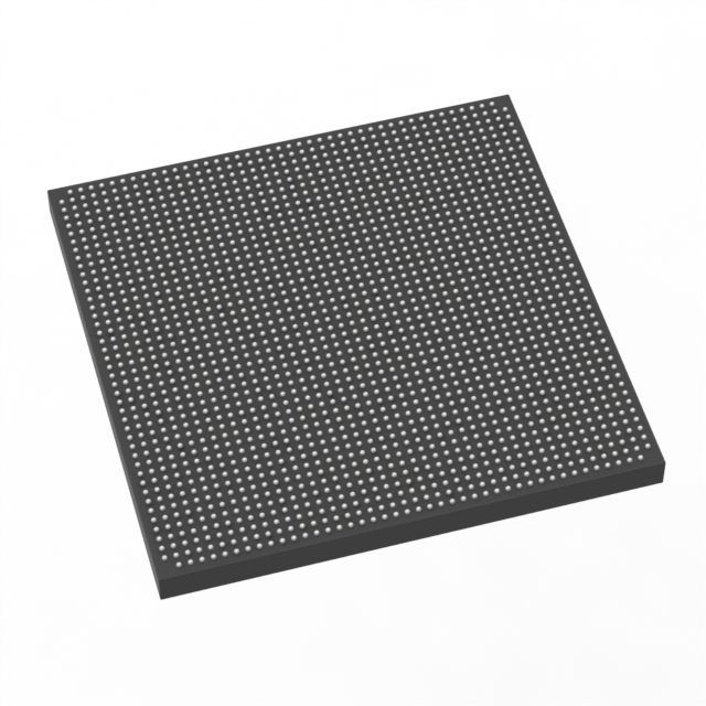
Arria 10 GX Field Programmable Gate Array (FPGA) IC 624 68857856 1150000 1932-BBGA, FCBGA |
|---|---|
| Quantity | 1,409 Available (as of June 14, 2026) |

| Product Category | Field Programmable Gate Array (FPGA) |
|---|---|
| Manufacturer | Intel |
| Manufacturing Status | Active |
| Manufacturer Standard Lead Time | 16 Weeks |
| Datasheet |
Specifications & Environmental
| Device Package | 1932-FCBGA (45x45) | Grade | Extended | Operating Temperature | 0°C – 100°C | ||
|---|---|---|---|---|---|---|---|
| Package / Case | 1932-BBGA, FCBGA | Number of I/O | 624 | Voltage | 870 mV - 930 mV | ||
| Mounting Method | Surface Mount | RoHS Compliance | RoHS Compliant | REACH Compliance | REACH Unaffected | ||
| Moisture Sensitivity Level | 3 (168 Hours) | Number of LABs/CLBs | 427200 | Number of Logic Elements/Cells | 1150000 | ||
| Number of Gates | N/A | ECCN | 3A001A7A | HTS Code | 8542.39.0001 | ||
| Qualification | N/A | Total RAM Bits | 68857856 |
Overview of 10AX115S3F45E2LG – Arria 10 GX Field Programmable Gate Array (FPGA) IC 624 68857856 1150000 1932-BBGA, FCBGA
The 10AX115S3F45E2LG is an Intel Arria 10 GX field programmable gate array (FPGA) in a 1932-FCBGA (45×45) package. It offers a mid-range, high-performance 20 nm FPGA architecture intended for applications that require large logic capacity, abundant on-chip memory, and extensive I/O connectivity.
Targeted markets include wireless and wireline communications, broadcast, computing and storage, medical imaging, and defense systems. Key value propositions highlighted in the device family documentation include higher performance versus prior mid-range devices and power efficiency enabled by on-device power-saving technologies.
Key Features
- Core Logic 1,150,000 logic elements provide substantial programmable logic capacity for complex logic and control functions.
- Embedded Memory 68,857,856 total RAM bits for on-chip buffering, caches, and data-path storage.
- I/O Capacity 624 general-purpose I/Os to support dense board-level connectivity and multiple external interfaces.
- Transceivers and Interfaces Arria 10 GX device family documentation lists support for high-speed serial transceivers and protocol hard IP, including PCIe Gen1/Gen2/Gen3 and 10 Gbps Ethernet-related features.
- DSP and Signal Processing Variable-precision DSP blocks are included in the Arria 10 family for compute-intensive signal-processing workloads.
- Clocking and PLLs Dedicated clock networks and PLL clock sources (including fractional synthesis and I/O PLLs) enable flexible clocking and timing architectures.
- Configuration and Reliability Device family supports dynamic and partial reconfiguration, enhanced configuration options, and SEU error detection and correction features as documented for the Arria 10 series.
- Package, Power and Thermal 1932-FCBGA (45×45) surface-mount package; voltage supply range 870 mV to 930 mV; operating temperature 0°C to 100°C. Device is RoHS compliant and is offered in Extended grade.
Typical Applications
- Wireless Infrastructure Channel and switch cards in remote radio heads and mobile backhaul systems leveraging high logic density and DSP resources.
- High‑Speed Wireline Line cards, muxponders and transponders for 40G/100G transport where integrated transceivers and protocol hard IP are useful.
- Broadcast and Professional AV Studio switches and video processing systems that require large on-chip memory and flexible I/O routing.
- Computing and Storage Acceleration Server acceleration functions, flash cache controllers and cloud compute offload using abundant logic and memory resources.
- Medical and Defense Systems Diagnostic imaging, radar, and electronic warfare subsystems that benefit from high logic capacity, DSP acceleration, and partial reconfiguration.
Unique Advantages
- High Logic Density: 1,150,000 logic elements enable complex designs and large-scale integration on a single device.
- Large On‑Chip Memory: 68,857,856 RAM bits support deep buffering, data-path storage, and memory-hungry algorithms without relying solely on external memory.
- Extensive I/O Count: 624 I/Os allow for broad connectivity to peripherals, transceivers, and board-level interfaces.
- Targeted High‑Speed Interfaces: Family-level support for PCIe Gen1/2/3, 10 Gbps Ethernet, and low-power serial transceivers simplifies integration of high-bandwidth links.
- Flexible Clocking and Reconfiguration: Dedicated clock networks, PLL options, and support for dynamic/partial reconfiguration facilitate complex timing domains and in-field updates.
- Extended Grade and RoHS Compliance: Extended-grade device with 0°C to 100°C operating range and RoHS compliance for a range of commercial and mission-oriented applications.
Why Choose 10AX115S3F45E2LG?
The 10AX115S3F45E2LG Arria 10 GX FPGA delivers substantial programmable logic, abundant embedded memory, and a high I/O count in a 1932-FCBGA package—making it well suited for mid-range designs that need a balance of performance and power efficiency. As part of the Intel Arria 10 family, the device benefits from documented architecture features such as variable-precision DSP blocks, rich clocking/PLL resources, and protocol hard IP support.
This combination positions the 10AX115S3F45E2LG for applications in communications, broadcast, compute acceleration, medical imaging, and defense systems where on-chip resources, flexible interfaces, and in-field reconfiguration are required. The Extended-grade offering and defined voltage and temperature ranges provide clear design constraints for system integration.
Request a quote or submit a product inquiry to receive pricing, lead time, and availability for the 10AX115S3F45E2LG Arria 10 GX FPGA.


Date Founded: 1968
Headquarters: Santa Clara, California, USA
Employees: 130,000+
Revenue: $54.23 Billion
Certifications and Memberships: ISO9001:2015, ISO14001:2015, ISO17025:2017, ISO27001:2022, ISO45001:2018, ISO50001:2018


