
10AX115S3F45I2SGES
| Part Description |
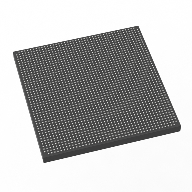
Arria 10 GX Field Programmable Gate Array (FPGA) IC 624 68857856 1150000 1932-BBGA, FCBGA |
|---|---|
| Quantity | 175 Available (as of June 18, 2026) |
| Product Category | Field Programmable Gate Array (FPGA) |
|---|---|
| Manufacturer | Intel |
| Manufacturing Status | Discontinued |
| Manufacturer Standard Lead Time | 9 Weeks |
| Datasheet |
Specifications & Environmental
| Device Package | 1932-FCBGA (45x45) | Grade | Industrial | Operating Temperature | -40°C – 100°C | ||
|---|---|---|---|---|---|---|---|
| Package / Case | 1932-BBGA, FCBGA | Number of I/O | 624 | Voltage | 870 mV - 930 mV | ||
| Mounting Method | Surface Mount | RoHS Compliance | RoHS Compliant | REACH Compliance | REACH Unaffected | ||
| Moisture Sensitivity Level | 3 (168 Hours) | Number of LABs/CLBs | 427200 | Number of Logic Elements/Cells | 1150000 | ||
| Number of Gates | N/A | ECCN | 3A001A7A | HTS Code | 8542.39.0001 | ||
| Qualification | N/A | Total RAM Bits | 68857856 |
Overview of 10AX115S3F45I2SGES – Arria 10 GX FPGA, 1,150,000 Logic Elements, 1932-FCBGA
The 10AX115S3F45I2SGES is an Intel Arria 10 GX field programmable gate array (FPGA) device built on a 20 nm mid-range FPGA architecture. It combines high logic capacity, substantial embedded RAM, and a large I/O count to address power-sensitive, high-performance applications across wireless, wireline, broadcast, computing, medical, and military markets.
Designed for systems that require scalable programmable logic, on-chip memory and robust I/O integration, this industrial-grade device delivers a balance of performance and efficiency with support for advanced features documented across the Arria 10 device family.
Key Features
- Core Logic — 1,150,000 logic elements provide extensive programmable resources for complex digital functions and large-scale logic integration.
- Programmable Logic Blocks — 427,200 LAB/CLB equivalents provide a flexible routing and logic fabric for custom architectures and IP integration.
- Embedded Memory — 68,857,856 total RAM bits on-chip to support large buffering, caching, and on-FPGA data structures.
- I/O Density — 624 user I/O pins enable broad external interfacing for high-bandwidth data paths and multi-channel connectivity.
- Package & Mounting — Available in a 1932-BBGA (1932-FCBGA, 45×45) package designed for surface-mount assembly to accommodate high pin counts in compact footprints.
- Power — Core voltage supply range of 870 mV to 930 mV, aligning with low-voltage, power-sensitive system designs.
- Operating Range — Industrial temperature grade with operating range from −40 °C to 100 °C for extended-environment deployments.
- Arria 10 Family Capabilities — Series-level features include support for external memory interfaces, PCIe Gen1/Gen2/Gen3 hard IP, enhanced PCS hard IP for high-speed protocols, low-power serial transceivers, dynamic and partial reconfiguration, and comprehensive clocking resources.
Typical Applications
- Wireless Infrastructure — Channel cards and remote radio head functions where high logic density and on-chip memory support signal processing and mobile backhaul tasks.
- Wireline Networking — Line cards, muxponders and transponders for 40G/100G systems that require high I/O count and protocol hard IP.
- Broadcast & Pro AV — Studio switching, transport and videoconferencing equipment that demand flexible I/O and on-FPGA buffering.
- Computing & Storage — Server acceleration, flash cache and cloud infrastructure elements leveraging large embedded memory and reconfigurable logic.
- Medical & Defense Systems — Diagnostic imaging, radar and secure communications applications benefiting from industrial temperature range and extensive logic resources.
Unique Advantages
- High Logic Capacity: 1,150,000 logic elements enable integration of complex custom logic and multiple IP blocks on a single device, reducing system BOM and board-level complexity.
- Substantial On-Chip Memory: Nearly 69 million bits of embedded RAM support large buffering and low-latency data paths without external memory for many functions.
- Large I/O and Dense Packaging: 624 I/O pins in a 1932-FCBGA (45×45) package provide the pin count needed for multi-channel interfaces and high-bandwidth connectivity.
- Power-Aware Design: 870–930 mV supply window and Arria 10 family power-saving technologies help optimize system power for energy-sensitive applications.
- Industrial Temperature Range: Rated −40 °C to 100 °C for reliable operation in extended-environment and industrial deployments.
- Family-Level Integration: Arria 10 features such as PCIe hard IP, support for high-speed serial protocols, and dynamic reconfiguration help accelerate time to market and enable advanced system architectures.
Why Choose 10AX115S3F45I2SGES?
The 10AX115S3F45I2SGES positions itself as a high-capacity, power-conscious midrange FPGA for applications that require a combination of dense logic, ample on-chip RAM, and broad I/O connectivity. As a member of the Intel Arria 10 family, it inherits device-level capabilities for high-speed interfaces, reconfiguration and system-level power management that help designers scale and evolve their platforms.
This device is suited to engineers and system designers building communications, compute acceleration, imaging, and secure or defense-oriented systems where industrial temperature support, high logic/memory resources and extensive external interfacing are key decision drivers.
Request a quote or submit a purchasing inquiry to get pricing, availability, and lead-time information for the 10AX115S3F45I2SGES.


Date Founded: 1968
Headquarters: Santa Clara, California, USA
Employees: 130,000+
Revenue: $54.23 Billion
Certifications and Memberships: ISO9001:2015, ISO14001:2015, ISO17025:2017, ISO27001:2022, ISO45001:2018, ISO50001:2018


