
10M02SCE144C8G
| Part Description |
MAX® 10 Field Programmable Gate Array (FPGA) IC 101 110592 2000 144-LQFP Exposed Pad |
|---|---|
| Quantity | 1,781 Available (as of June 9, 2026) |

| Product Category | Field Programmable Gate Array (FPGA) |
|---|---|
| Manufacturer | Intel |
| Manufacturing Status | Active |
| Manufacturer Standard Lead Time | 16 Weeks |
| Datasheet |
Specifications & Environmental
| Device Package | 144-EQFP (20x20) | Grade | Commercial | Operating Temperature | 0°C – 85°C | ||
|---|---|---|---|---|---|---|---|
| Package / Case | 144-LQFP Exposed Pad | Number of I/O | 101 | Voltage | 2.85 V - 3.465 V | ||
| Mounting Method | Surface Mount | RoHS Compliance | RoHS Compliant | REACH Compliance | REACH Unaffected | ||
| Moisture Sensitivity Level | 3 (168 Hours) | Number of LABs/CLBs | 125 | Number of Logic Elements/Cells | 2000 | ||
| Number of Gates | N/A | ECCN | 3A991D | HTS Code | 8542.39.0001 | ||
| Qualification | N/A | Total RAM Bits | 110592 |
Overview of 10M02SCE144C8G – MAX® 10 FPGA, 2,000 Logic Elements, 144-LQFP Exposed Pad
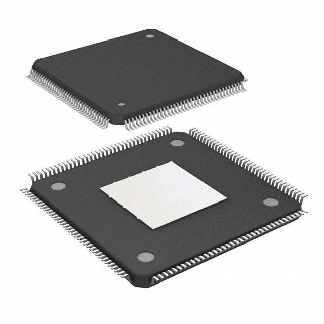
The 10M02SCE144C8G is a MAX® 10 Field Programmable Gate Array (FPGA) IC from Intel, supplied in a 144-LQFP exposed pad package. It provides a compact, surface-mount FPGA option with 2,000 logic elements, 110,592 bits of embedded RAM and 101 user I/O pins.
Designed for commercial-temperature embedded designs, this device operates from a 2.85 V to 3.465 V supply and is specified for 0 °C to 85 °C, making it suitable for a broad range of general-purpose control, interface and glue-logic applications where moderate logic density and on-chip RAM are required.
Key Features
- Core Logic: 2,000 logic elements and 125 logic array blocks provide the programmable fabric for implementing custom digital functions and glue logic.
- Memory: 110,592 bits of total on-chip RAM to store FIFOs, small buffers or state data without external memory.
- I/O Capacity: 101 user I/O pins to support multiple interfaces, GPIO and peripheral connections in a single-package solution.
- Package & Mounting: 144-LQFP exposed pad (supplier device package: 144-EQFP, 20 × 20) in a surface-mount form factor to ease board-level integration and thermal conduction via the exposed pad.
- Power: Specified operating supply range of 2.85 V to 3.465 V to match common system rails.
- Temperature & Grade: Commercial grade operation across 0 °C to 85 °C for typical consumer and industrial-adjacent applications.
- Environmental Compliance: RoHS compliant for assembly and end-product regulatory needs.
Typical Applications
- Embedded Control: Implement control logic and state machines using the device’s 2,000 logic elements and on-chip RAM for local storage.
- Interface and Glue Logic: Consolidate multiple interface buffers and protocol adaptors using the 101 I/O pins to reduce board-level component count.
- Human-Machine Interfaces: Drive and manage displays, buttons and peripheral sensors where moderate I/O and on-chip memory are required.
Unique Advantages
- Right-sized Logic Density: 2,000 logic elements deliver sufficient capability for control, interface and small-scale datapath designs without over-specifying resources.
- Integrated RAM: 110,592 bits of on-chip RAM reduce reliance on external memory, simplifying BOM and board routing.
- Generous I/O Count: 101 I/O pins allow flexible connectivity to peripherals and multiple interfaces from a single device.
- Compact Surface-Mount Package: The 144-LQFP exposed pad package supports compact PCB layouts and improved thermal path for the device.
- Commercial Temperature Rating: Rated for 0 °C to 85 °C to match standard commercial product requirements.
- RoHS Compliant: Meets RoHS requirements to support restricted-substance compliance in assemblies.
Why Choose 10M02SCE144C8G?
The 10M02SCE144C8G positions itself as a compact, commercially graded FPGA option that balances logic capacity, on-chip RAM and I/O count in a single surface-mount package. It is well suited to designers who need embedded programmable logic for control, interface consolidation or HMI tasks while maintaining a small board footprint and standard supply voltage compatibility.
Backed by Intel’s MAX® 10 family designation and RoHS compliance, this device offers a straightforward migration path for projects that require modest logic resources, integrated RAM, and a 144-LQFP exposed pad package for efficient PCB integration.
Request a quote or submit an inquiry to obtain pricing and availability for the 10M02SCE144C8G and to discuss volume or delivery options for your design needs.


Date Founded: 1968
Headquarters: Santa Clara, California, USA
Employees: 130,000+
Revenue: $54.23 Billion
Certifications and Memberships: ISO9001:2015, ISO14001:2015, ISO17025:2017, ISO27001:2022, ISO45001:2018, ISO50001:2018


