
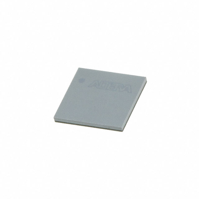
10M02DCV36C8G
| Part Description |
MAX® 10 Field Programmable Gate Array (FPGA) IC 27 110592 2000 36-UFBGA, WLCSP |
|---|---|
| Quantity | 487 Available (as of October 7, 2026) |
| Product Category | Field Programmable Gate Array (FPGA) |
|---|---|
| Manufacturer | Intel |
| Manufacturing Status | Active |
| Manufacturer Standard Lead Time | 16 Weeks |
| Datasheet |
Specifications & Environmental
| Device Package | 36-VBGA (3.47x3.4) | Grade | Commercial | Operating Temperature | 0°C – 85°C | ||
|---|---|---|---|---|---|---|---|
| Package / Case | 36-UFBGA, WLCSP | Number of I/O | 27 | Voltage | 1.15 V - 1.25 V | ||
| Mounting Method | Surface Mount | RoHS Compliance | RoHS Compliant | REACH Compliance | REACH Unaffected | ||
| Moisture Sensitivity Level | 1 (Unlimited) | Number of LABs/CLBs | 125 | Number of Logic Elements/Cells | 2000 | ||
| Number of Gates | N/A | ECCN | 3A991D | HTS Code | 8542.39.0001 | ||
| Qualification | N/A | Total RAM Bits | 110592 |
Overview of 10M02DCV36C8G – MAX® 10 Field Programmable Gate Array (FPGA) IC 27 110592 2000 36-UFBGA, WLCSP
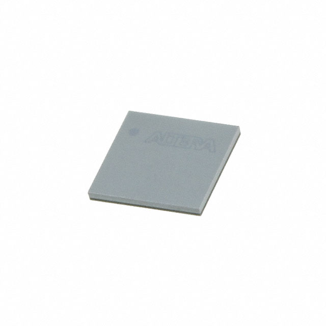
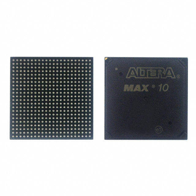
The 10M02DCV36C8G is an Intel MAX® 10 field programmable gate array supplied in a 36‑UFBGA/WLCSP package. It provides a compact, commercial‑grade FPGA option with 2,000 logic elements, 110,592 total RAM bits and 27 general-purpose I/Os for small to mid-density programmable logic tasks.
Designed for surface‑mount applications, this device operates from a 1.15 V to 1.25 V supply and across a commercial temperature range of 0 °C to 85 °C. The device is RoHS compliant and is documented in the Intel MAX 10 FPGA device datasheet.
Key Features
- Logic Capacity 2,000 logic elements provide a predictable resource footprint for control logic, glue logic, and compact programmable functions.
- On‑chip Memory 110,592 total RAM bits to support small FIFOs, buffers, and temporary data storage within the FPGA fabric.
- Input/Output 27 I/Os to interface with external peripherals, sensors, and other digital devices.
- Power Supply Operating voltage range of 1.15 V to 1.25 V for core supply planning and power budgeting.
- Package and Mounting 36‑UFBGA (WLCSP) package; supplier device package listed as 36‑VBGA (3.47 × 3.4 mm) for compact PCB integration. Surface mount device suitable for standard assembly.
- Commercial Grade Rated for 0 °C to 85 °C operation; suitable for temperature environments within commercial specifications.
- Regulatory RoHS compliant.
Typical Applications
- Embedded control and logic Compact control engines and sequencers that fit within a 2,000 logic‑element budget and require on‑chip RAM.
- Sensor and peripheral interfacing Interface glue between sensors, ADC/DAC front ends, and host controllers using the available 27 I/Os.
- Custom peripheral implementation Small custom peripherals, protocol bridging, and timing-critical glue logic where a compact FPGA package is required.
- Evaluation and prototyping Low‑density designs and proof‑of‑concept implementations that benefit from integrated RAM and a small‑form‑factor BGA/WLCSP package.
Unique Advantages
- Compact, low‑profile package: The 36‑UFBGA/WLCSP footprint (36‑VBGA, 3.47 × 3.4 mm) enables space‑constrained PCB designs without sacrificing programmable logic capability.
- Balanced logic and memory mix: 2,000 logic elements combined with 110,592 RAM bits provide a practical balance for control, buffering, and simple data processing tasks.
- Predictable power envelope: Defined core supply range of 1.15 V to 1.25 V simplifies power supply design and system integration.
- Commercial temperature support: Rated for 0 °C to 85 °C operation for standard commercial applications.
- RoHS compliant: Meets RoHS environmental requirements for lead‑free assembly and global regulatory needs.
Why Choose 10M02DCV36C8G?
The 10M02DCV36C8G delivers a concise combination of logic, memory, and I/O in a very small package, making it a practical choice for designs that require programmable logic without large FPGA resources. Its commercial temperature rating and defined supply range make it straightforward to integrate into space‑limited consumer and industrial control boards where moderate logic capacity and on‑chip RAM are sufficient.
Backed by the Intel MAX 10 device documentation, this part is positioned for developers and procurement teams seeking a verified, compact FPGA solution that balances integration, size, and predictable electrical specifications.
Request a quote or submit an inquiry to get pricing, availability, and assistance integrating the 10M02DCV36C8G into your design.






















Date Founded: 1968
Headquarters: Santa Clara, California, USA
Employees: 130,000+
Revenue: $54.23 Billion
Certifications and Memberships: ISO9001:2015, ISO14001:2015, ISO17025:2017, ISO27001:2022, ISO45001:2018, ISO50001:2018


