
10M02SCE144C7G
| Part Description |
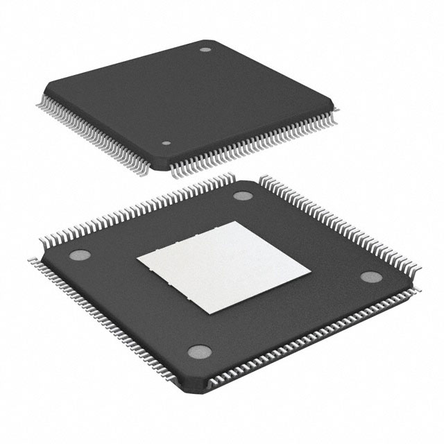
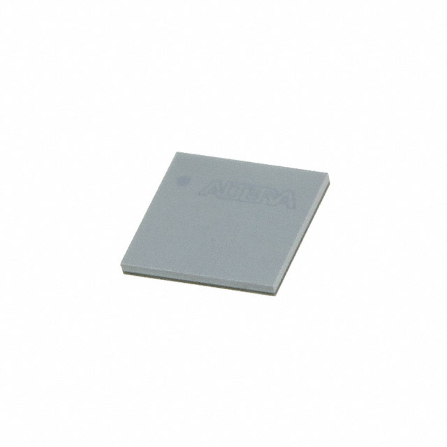
MAX® 10 Field Programmable Gate Array (FPGA) IC 101 110592 2000 144-LQFP Exposed Pad |
|---|---|
| Quantity | 713 Available (as of October 8, 2026) |
| Product Category | Field Programmable Gate Array (FPGA) |
|---|---|
| Manufacturer | Intel |
| Manufacturing Status | Obsolete |
| Manufacturer Standard Lead Time | Contact Us |
| Datasheet |
Specifications & Environmental
| Device Package | 144-EQFP (20x20) | Grade | Commercial | Operating Temperature | 0°C – 85°C | ||
|---|---|---|---|---|---|---|---|
| Package / Case | 144-LQFP Exposed Pad | Number of I/O | 101 | Voltage | 2.85 V - 3.465 V | ||
| Mounting Method | Surface Mount | RoHS Compliance | Unknown | REACH Compliance | REACH Unknown | ||
| Moisture Sensitivity Level | 3 (168 Hours) | Number of LABs/CLBs | 125 | Number of Logic Elements/Cells | 2000 | ||
| Number of Gates | N/A | ECCN | 3A991D | HTS Code | 8542.39.0001 | ||
| Qualification | N/A | Total RAM Bits | 110592 |
Overview of 10M02SCE144C7G – MAX® 10 FPGA (144‑LQFP Exposed Pad)
The 10M02SCE144C7G is an Intel MAX® 10 field programmable gate array (FPGA) in a 144‑LQFP exposed‑pad surface‑mount package. This commercial‑grade device provides a compact FPGA fabric with 2,000 logic elements, 110,592 bits of on‑chip RAM, and 101 user I/O pins for medium‑complexity embedded designs.
Designed for systems that require integrated programmable logic, on‑chip memory, and a moderate I/O count, the device operates from a 2.85 V to 3.465 V supply and across a 0 °C to 85 °C commercial temperature range. It is RoHS compliant and shipped in a 144‑pin LQFP (20 × 20) form factor with an exposed pad for board mounting.
Key Features
- FPGA Core 2,000 logic elements provide programmable logic resources for implementing custom digital functions and control logic.
- On‑chip Memory 110,592 total RAM bits enable local buffering, state retention, and small‑to‑moderate data storage without external memory.
- I/O Capacity 101 user I/O pins support interfacing to sensors, peripherals, and board‑level logic while keeping form factor compact.
- Power Supply Operates from a 2.85 V to 3.465 V supply range, suitable for common system voltage rails.
- Package & Mounting 144‑LQFP exposed pad (supplier package: 144‑EQFP 20×20) in a surface‑mount configuration for PCB space efficiency and thermal conduction to the board.
- Temperature & Grade Commercial grade with an operating temperature range of 0 °C to 85 °C for standard consumer and embedded environments.
- Standards Compliance RoHS compliant to support environmentally conscious designs.
- Documentation Part of the Intel MAX 10 FPGA family with published device datasheet content covering electrical, switching, and configuration specifications.
Typical Applications
- Embedded Control Implement custom control logic, finite state machines, and glue logic where 2,000 logic elements and local RAM meet system requirements.
- Consumer Electronics Use the device for user‑interface control, peripheral aggregation, and on‑board signal processing in space‑constrained designs.
- IoT & Edge Devices Deploy as a compact programmable logic element to handle sensor interfacing, pre‑processing, and protocol bridging with 101 available I/Os.
- Prototyping & Development Leverage the MAX 10 device’s documented electrical and timing specifications for early functional prototyping and small production runs.
Unique Advantages
- Balanced Logic & Memory: 2,000 logic elements paired with 110,592 RAM bits provide a balanced resource mix for control logic plus on‑chip data storage without external components.
- Sufficient I/O for Mixed Interfaces: 101 user I/Os allow integration of multiple peripherals and interfaces on a single device, reducing board complexity.
- Compact, Serviceable Package: 144‑LQFP exposed pad format offers a compact footprint with an exposed pad for improved thermal conduction to the PCB.
- Commercial‑Grade Operating Range: 0 °C to 85 °C operation aligns with consumer and many embedded application environments.
- Clear Electrical Boundaries: Defined supply range (2.85 V–3.465 V) and published datasheet material make power and timing planning straightforward during design.
- RoHS Compliance: Environmentally compliant finish supports green product initiatives and regulatory needs.
Why Choose 10M02SCE144C7G?
The 10M02SCE144C7G positions itself as a compact, documented MAX 10 FPGA option for designers who need moderate logic capacity, substantial on‑chip RAM, and a generous I/O count in a surface‑mount 144‑pin package. Its defined electrical and thermal parameters simplify integration into consumer and embedded systems running from standard 3.3 V rails.
This part is appropriate for teams seeking a commercial‑grade programmable logic device with RoHS compliance and published Intel MAX 10 datasheet material to support electrical, switching, and configuration planning during development and production.
Request a quote or contact sales to obtain pricing, availability, and lead‑time information for 10M02SCE144C7G.
























Date Founded: 1968
Headquarters: Santa Clara, California, USA
Employees: 130,000+
Revenue: $54.23 Billion
Certifications and Memberships: ISO9001:2015, ISO14001:2015, ISO17025:2017, ISO27001:2022, ISO45001:2018, ISO50001:2018


