
10M02SCM153C8G
| Part Description |
MAX® 10 Field Programmable Gate Array (FPGA) IC 112 110592 2000 153-VFBGA |
|---|---|
| Quantity | 1,139 Available (as of June 10, 2026) |

| Product Category | Field Programmable Gate Array (FPGA) |
|---|---|
| Manufacturer | Intel |
| Manufacturing Status | Active |
| Manufacturer Standard Lead Time | 16 Weeks |
| Datasheet |
Specifications & Environmental
| Device Package | 153-MBGA (8x8) | Grade | Commercial | Operating Temperature | 0°C – 85°C | ||
|---|---|---|---|---|---|---|---|
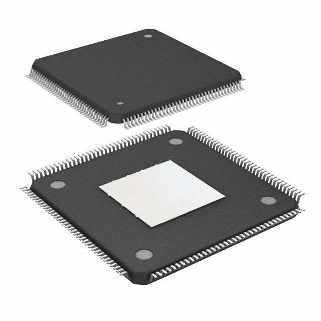
| Package / Case | 153-VFBGA | Number of I/O | 112 | Voltage | 2.85 V - 3.465 V | ||
| Mounting Method | Surface Mount | RoHS Compliance | RoHS Compliant | REACH Compliance | REACH Unaffected | ||
| Moisture Sensitivity Level | 3 (168 Hours) | Number of LABs/CLBs | 125 | Number of Logic Elements/Cells | 2000 | ||
| Number of Gates | N/A | ECCN | 3A991D | HTS Code | 8542.39.0001 | ||
| Qualification | N/A | Total RAM Bits | 110592 |
Overview of 10M02SCM153C8G – MAX® 10 FPGA, 2,000 logic elements, 153‑VFBGA
The 10M02SCM153C8G is a MAX® 10 Field Programmable Gate Array (FPGA) IC from Intel, packaged in a 153‑VFBGA (153‑MBGA, 8×8) surface‑mount package. It delivers a mid‑density FPGA fabric with 2,000 logic elements, 110,592 bits of on‑chip RAM and up to 112 user I/O lines.
Designed for commercial‑grade systems, this device targets designs that require configurable logic, embedded RAM and flexible I/O in a compact surface‑mount form factor. Key value comes from its combination of on‑chip memory, I/O count and a supply voltage range compatible with common 3.3 V systems.
Key Features
- Logic resources — 2,000 logic elements provide the core programmable fabric for custom logic, control and glue‑logic functions.
- On‑chip memory — 110,592 total RAM bits for local buffering, FIFOs and small embedded data structures without external memory.
- I/O — 112 user I/O pins to interface with peripherals, sensors and other system components.
- Power — Supports a voltage supply range of 2.85 V to 3.465 V, aligning with typical 3.3 V logic domains.
- Package and mounting — 153‑VFBGA (supplier package 153‑MBGA, 8×8) in a surface‑mount form factor for compact PCB layouts and automated assembly.
- Operational grade and temperature — Commercial grade device rated for 0 °C to 85 °C operation.
- Environmental compliance — RoHS compliant for regulatory alignment in commercial products.
Typical Applications
- Commercial embedded systems — Implement custom control logic and I/O aggregation in compact commercial devices using the device’s logic elements and 112 I/O lines.
- Protocol bridging and interface adaptation — Use on‑chip RAM for packet buffering and logic elements to translate between peripheral interfaces or handle protocol conversion.
- Human‑machine interfaces (HMI) — Manage button scanning, LED driving and simple display/indicator control while offloading tasks from the main processor.
Unique Advantages
- Balanced mid‑density logic — 2,000 logic elements provide a good fit for designs that need more capability than small CPLDs but do not require high‑end FPGA densities.
- Integrated on‑chip RAM — 110,592 bits of RAM reduce the need for external memory for buffering and small data structures, simplifying BOM and PCB routing.
- Ample I/O count — 112 user I/O lines enable direct connections to multiple peripherals and sensors without external multiplexing.
- Compact surface‑mount package — 153‑VFBGA (8×8) supports space‑constrained designs and standard automated assembly processes.
- Commercial temperature rating — 0 °C to 85 °C operation and RoHS compliance align the device with a wide range of commercial‑grade product requirements.
- 3.3 V domain compatibility — 2.85 V to 3.465 V supply range fits common 3.3 V system designs for straightforward integration.
Why Choose 10M02SCM153C8G?
The 10M02SCM153C8G positions itself as a compact, commercial‑grade FPGA solution from Intel’s MAX® 10 family, offering a combination of 2,000 logic elements, substantial on‑chip RAM and 112 I/O pins in a 153‑VFBGA surface‑mount package. Its electrical and thermal ratings make it suitable for a broad set of commercial embedded designs that need configurable logic and local memory without the complexity or cost of larger FPGAs.
This device is well suited to engineers and product teams building mid‑density logic functions, peripheral bridging, or HMI controllers who require a balance of integration, board‑area efficiency and straightforward 3.3 V system compatibility.
Request a quote or submit a product inquiry for 10M02SCM153C8G to receive pricing and availability details for your next design.


Date Founded: 1968
Headquarters: Santa Clara, California, USA
Employees: 130,000+
Revenue: $54.23 Billion
Certifications and Memberships: ISO9001:2015, ISO14001:2015, ISO17025:2017, ISO27001:2022, ISO45001:2018, ISO50001:2018


