
10M02DCV36I7G
| Part Description |
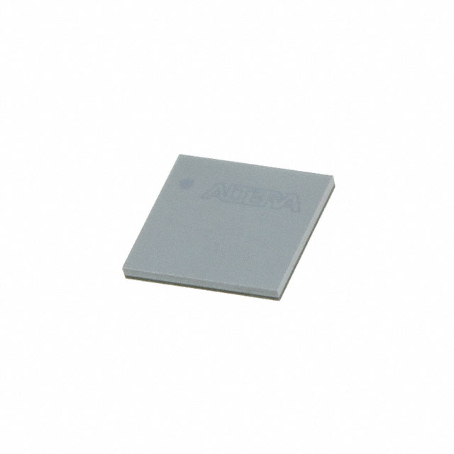
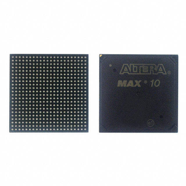
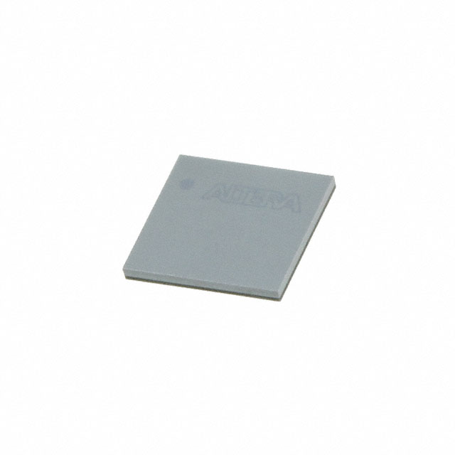
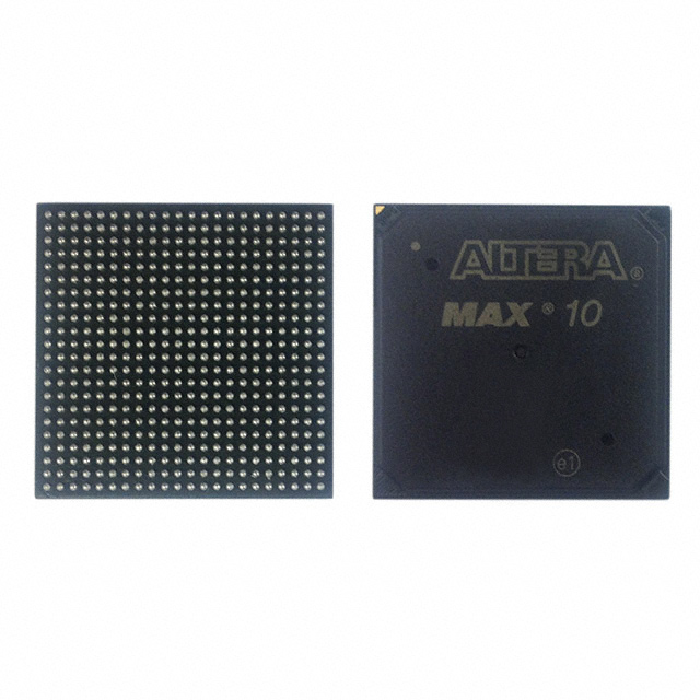
MAX® 10 Field Programmable Gate Array (FPGA) IC 27 110592 2000 36-UFBGA, WLCSP |
|---|---|
| Quantity | 1,810 Available (as of October 8, 2026) |
| Product Category | Field Programmable Gate Array (FPGA) |
|---|---|
| Manufacturer | Intel |
| Manufacturing Status | Active |
| Manufacturer Standard Lead Time | 16 Weeks |
| Datasheet |
Specifications & Environmental
| Device Package | 36-VBGA (3.47x3.4) | Grade | Industrial | Operating Temperature | -40°C – 100°C | ||
|---|---|---|---|---|---|---|---|
| Package / Case | 36-UFBGA, WLCSP | Number of I/O | 27 | Voltage | 1.15 V - 1.25 V | ||
| Mounting Method | Surface Mount | RoHS Compliance | RoHS Compliant | REACH Compliance | REACH Unaffected | ||
| Moisture Sensitivity Level | 1 (Unlimited) | Number of LABs/CLBs | 125 | Number of Logic Elements/Cells | 2000 | ||
| Number of Gates | N/A | ECCN | EAR99 | HTS Code | 8542.39.0001 | ||
| Qualification | N/A | Total RAM Bits | 110592 |
Overview of 10M02DCV36I7G – MAX® 10 FPGA IC (36-UFBGA)
The 10M02DCV36I7G is an Intel MAX® 10 Field Programmable Gate Array (FPGA) provided in a 36‑UFBGA/WLCSP package. It offers a compact, industrial‑grade FPGA option with on‑chip RAM and a defined set of I/O suitable for space‑constrained embedded designs.
This device combines 2,000 logic elements and 110,592 bits of on‑chip RAM with 27 I/O pins, a 1.15 V–1.25 V core supply range, and an operating temperature range of −40 °C to 100 °C, making it suitable for industrial applications where compact size and predictable electrical characteristics are required.
Key Features
- Core logic — 2,000 logic elements (125 LABs) to implement small to mid‑scale logic functions and control logic.
- On‑chip memory — 110,592 total RAM bits for distributed storage, buffering, and small lookup tables without external memory.
- I/O — 27 user I/O pins to interface with peripherals, sensors, and simple bus structures.
- Power — Core voltage supply range of 1.15 V to 1.25 V to match system power rails and predictable power budgeting.
- Package & mounting — 36‑UFBGA WLCSP (supplier package: 36‑VBGA, 3.47 × 3.4 mm) in a surface‑mount form factor for compact PCB layouts.
- Temperature & grade — Industrial grade with an operating temperature range of −40 °C to 100 °C for deployment in outdoor or factory environments.
- Compliance — RoHS compliant.
Typical Applications
- Compact control systems — Implement control and sequencing logic where up to 2,000 logic elements and 110,592 bits of RAM meet functional requirements in a small footprint.
- Embedded interface hubs — Aggregate and translate signals using available 27 I/O pins for sensor interfaces and peripheral bridging in space‑limited designs.
- Industrial instrumentation — Deploy in instruments operating across −40 °C to 100 °C that require an industrial‑grade programmable logic device in a small package.
- Low‑footprint FPGA integration — Add programmable logic capability to compact PCBs where a WLCSP 36‑ball package (3.47 × 3.4 mm) is advantageous.
Unique Advantages
- Right‑sized logic capacity: 2,000 logic elements provide a balanced resource set for control, glue logic, and small accelerators without excess complexity.
- Significant on‑chip RAM: 110,592 bits of RAM reduce or eliminate the need for external memory for many buffering and lookup tasks, simplifying BOM and layout.
- Compact WLCSP package: The 36‑UFBGA (36‑VBGA, 3.47 × 3.4 mm) package minimizes PCB area and supports high‑density board designs.
- Industrial temperature range: Rated from −40 °C to 100 °C for reliable operation in harsher environmental conditions common to industrial deployments.
- Predictable power envelope: Defined core supply range (1.15 V–1.25 V) helps streamline power design and thermal planning for small systems.
- RoHS compliant: Conforms to common environmental requirements for global product assemblies.
Why Choose 10M02DCV36I7G?
The 10M02DCV36I7G provides a compact, industrial‑grade FPGA solution from Intel that balances logic density, on‑chip RAM, and I/O in a very small WLCSP package. Its combination of 2,000 logic elements, 110,592 bits of RAM, and a 27‑pin I/O count make it well suited to designs that require programmable logic capability without large form factors or complex power architectures.
This part is appropriate for designers seeking a small, rugged FPGA with predictable electrical and thermal characteristics. The device’s packaging and RoHS compliance support integration into space‑constrained PCBs and industrial product lines where long‑term availability and ecosystem support for MAX® 10 devices are important.
Request a quote or submit a pricing inquiry to receive availability and ordering information for 10M02DCV36I7G.























Date Founded: 1968
Headquarters: Santa Clara, California, USA
Employees: 130,000+
Revenue: $54.23 Billion
Certifications and Memberships: ISO9001:2015, ISO14001:2015, ISO17025:2017, ISO27001:2022, ISO45001:2018, ISO50001:2018


