
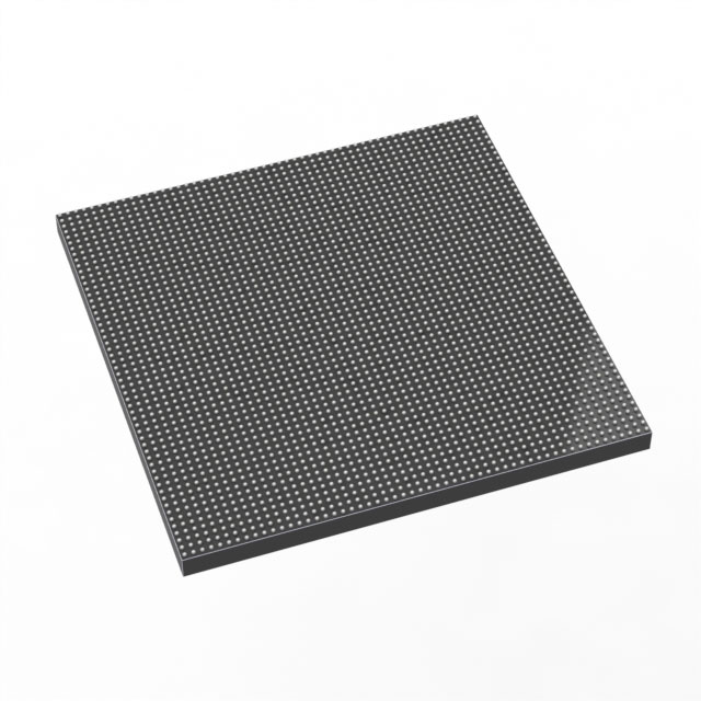
1ST280EY3F55E3XG
| Part Description |
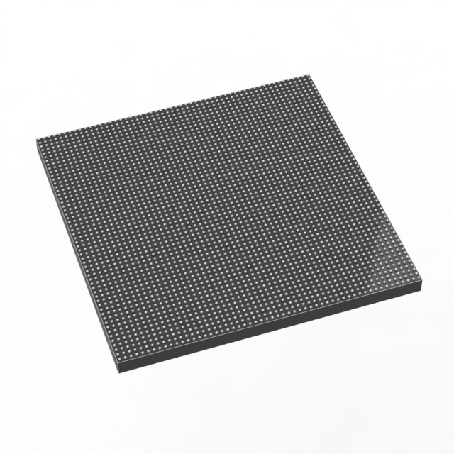
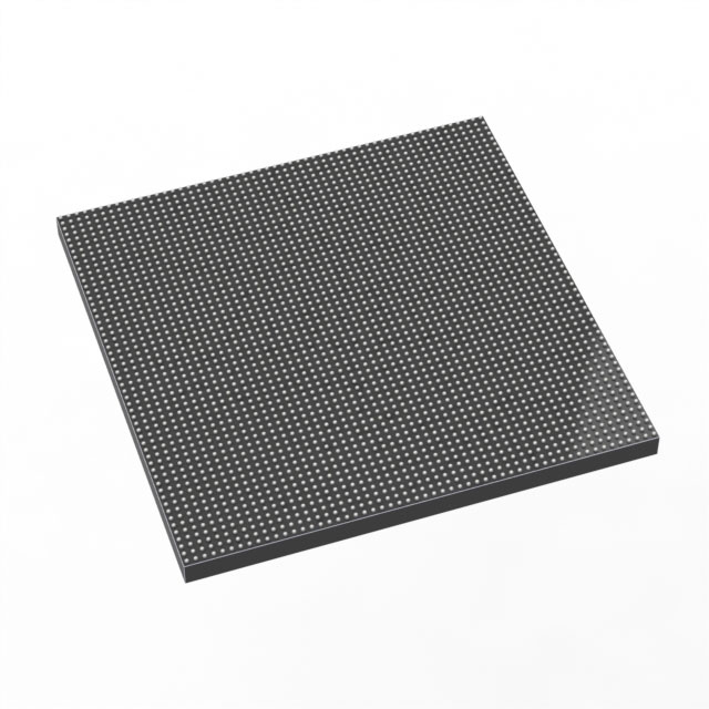
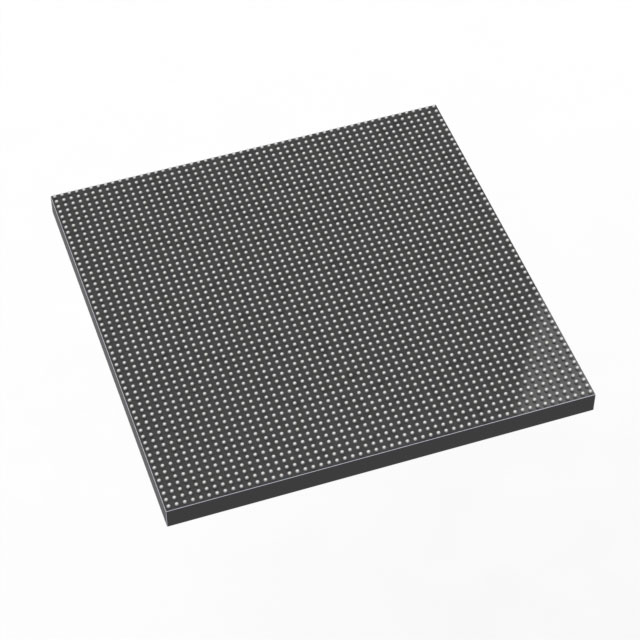
Stratix® 10 TX Field Programmable Gate Array (FPGA) IC 296 2800000 2912-BBGA, FCBGA |
|---|---|
| Quantity | 21 Available (as of October 7, 2026) |
| Product Category | Field Programmable Gate Array (FPGA) |
|---|---|
| Manufacturer | Intel |
| Manufacturing Status | Active |
| Manufacturer Standard Lead Time | 12 Weeks |
| Datasheet |
Specifications & Environmental
| Device Package | 2912-FBGA, FC (55x55) | Grade | Extended | Operating Temperature | 0°C – 100°C | ||
|---|---|---|---|---|---|---|---|
| Package / Case | 2912-BBGA, FCBGA | Number of I/O | 296 | Voltage | 820 mV - 880 mV | ||
| Mounting Method | Surface Mount | RoHS Compliance | Unknown | REACH Compliance | REACH Unaffected | ||
| Moisture Sensitivity Level | 3 (168 Hours) | Number of LABs/CLBs | 350000 | Number of Logic Elements/Cells | 2800000 | ||
| Number of Gates | N/A | ECCN | N/A | HTS Code | N/A | ||
| Qualification | N/A | Total RAM Bits | 240123904 |
Overview of 1ST280EY3F55E3XG – Stratix® 10 TX FPGA, 2.8M Logic Elements, 2912-BBGA
The 1ST280EY3F55E3XG is an Intel Stratix® 10 TX field programmable gate array (FPGA) delivered in a 2912‑BBGA FCBGA surface‑mount package. It integrates a high‑performance HyperFlex® core architecture and dense programmable fabric, offering 2,800,000 logic elements and extensive on‑chip RAM for demanding high‑bandwidth designs.
Designed for applications that require large programmable capacity and high transceiver throughput, this device targets networking, communications and compute acceleration markets where integration, performance, and power‑efficient signaling are primary concerns.
Key Features
- Core Performance HyperFlex® core architecture and a monolithic 14 nm FPGA fabric with 2,800,000 logic elements to support complex, high‑performance logic implementations.
- Memory Total on‑chip RAM of 240,123,904 bits, supplemented by internal M20K memory blocks and support for embedded eSRAM in select devices to handle large buffering and state storage requirements.
- High‑Speed Transceivers Dual‑mode transceivers capable of 57.8 Gbps PAM4 and 28.9 Gbps NRZ operation for chip‑to‑chip, chip‑to‑module, and backplane links (series feature).
- Hard IP Blocks Hardened PCI Express Gen3 and 10/25/100 Gbps Ethernet MAC IP blocks (series feature) to accelerate protocol implementations and reduce soft IP overhead.
- I/O and Package 296 I/Os in a 2912‑BBGA (FCBGA) package; supplier package listed as 2912‑FBGA, FC (55×55). Surface‑mount mounting type for dense board integration.
- Power and Operating Range Core supply voltage range of 820 mV to 880 mV and an operating temperature range of 0 °C to 100 °C, suitable for extended‑grade deployments.
- System and Security Features Series documentation references device configuration, Secure Device Manager (SDM), and device security features to support managed configuration and protected bitstreams.
- Compliance RoHS compliant.
Typical Applications
- High‑Bandwidth Networking Implement aggregation and line cards that require multi‑Tbps switching and hardened 10/25/100 Gbps Ethernet MACs with high‑speed transceiver support.
- Data Center Acceleration Offload and accelerate compute kernels with dense programmable fabric and large on‑chip RAM for buffering and stateful processing.
- Telecommunications Infrastructure Support backplane and chip‑to‑module links using dual‑mode transceivers for NRZ and PAM4 signaling in next‑generation transport systems.
- High‑Speed Test & Measurement Build signal processing and capture systems that need low‑latency logic, high I/O counts, and high‑rate serial interfaces.
Unique Advantages
- Highly Scalable Logic Capacity: 2,800,000 logic elements provide the programmable density required for complex algorithms and large‑scale integrations without immediate external logic augmentation.
- Integrated High‑Speed Connectivity: Dual‑mode transceivers and hardened protocol IP reduce design risk and accelerate time‑to‑market for multi‑Gbps links.
- Substantial On‑Chip Memory: 240,123,904 bits of RAM support extensive buffering, lookup tables, and state machines directly in the fabric to minimize external memory dependency.
- Compact, High‑Pin Package: 2912‑BBGA (55×55) package with 296 I/Os enables dense system designs and a high IO‑to‑package area ratio for complex boards.
- Extended‑Grade Operating Range: Rated for 0 °C to 100 °C and RoHS compliant, suitable for applications requiring extended temperature operation and environmental compliance.
Why Choose 1ST280EY3F55E3XG?
The 1ST280EY3F55E3XG brings the Stratix 10 TX family’s high‑performance HyperFlex architecture and advanced transceiver capabilities into a single, highly integrated FPGA package. With 2.8 million logic elements, large on‑chip RAM, hardened protocol IP options, and dual‑mode high‑speed serial interfaces, it is positioned for complex networking, compute acceleration, and telecommunications designs that demand both logic density and high aggregate bandwidth.
This device suits engineers and system architects who require a scalable, high‑capacity programmable platform with on‑board resources for heavy data movement and protocol acceleration, supported by Intel Stratix 10 TX device features and ecosystem resources.
Request a quote or contact sales to discuss availability, lead time, and pricing for the 1ST280EY3F55E3XG.





















Date Founded: 1968
Headquarters: Santa Clara, California, USA
Employees: 130,000+
Revenue: $54.23 Billion
Certifications and Memberships: ISO9001:2015, ISO14001:2015, ISO17025:2017, ISO27001:2022, ISO45001:2018, ISO50001:2018


