
5AGXBA3D4F27C5G
| Part Description |
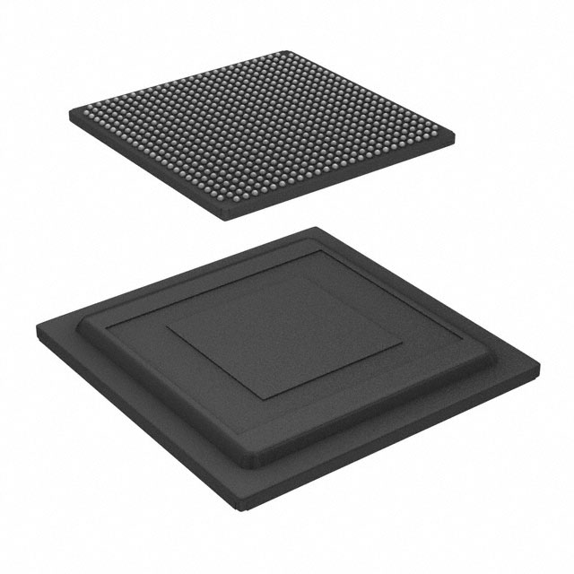
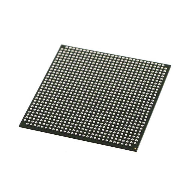
Arria V GX Field Programmable Gate Array (FPGA) IC 336 11746304 156000 672-BBGA, FCBGA |
|---|---|
| Quantity | 126 Available (as of June 15, 2026) |

| Product Category | Field Programmable Gate Array (FPGA) |
|---|---|
| Manufacturer | Intel |
| Manufacturing Status | Active |
| Manufacturer Standard Lead Time | 16 Weeks |
| Datasheet |
Specifications & Environmental
| Device Package | 672-FBGA (27x27) | Grade | Commercial | Operating Temperature | 0°C – 85°C | ||
|---|---|---|---|---|---|---|---|
| Package / Case | 672-BBGA, FCBGA | Number of I/O | 336 | Voltage | 1.07 V - 1.13 V | ||
| Mounting Method | Surface Mount | RoHS Compliance | RoHS Compliant | REACH Compliance | REACH Unaffected | ||
| Moisture Sensitivity Level | 3 (168 Hours) | Number of LABs/CLBs | 7362 | Number of Logic Elements/Cells | 156000 | ||
| Number of Gates | N/A | ECCN | PENDING ECCN | HTS Code | 0000.00.0000 | ||
| Qualification | N/A | Total RAM Bits | 11746304 |
Overview of 5AGXBA3D4F27C5G – Arria V GX FPGA IC, 156000 logic elements, 336 I/O
The 5AGXBA3D4F27C5G is an Arria V GX Field Programmable Gate Array (FPGA) supplied in a 672-BBGA FCBGA package. It delivers high on-chip logic and memory capacity combined with a substantial I/O count for complex, integration-heavy designs.
With 156,000 logic elements, 11,746,304 bits of embedded RAM and 336 general-purpose I/O, this commercial-grade device is tailored for designs that require significant programmable logic, on-chip memory bandwidth, and a dense I/O footprint while operating within standard commercial temperature and core-voltage envelopes.
Key Features
- Logic Capacity — 156,000 logic elements provide substantial programmable fabric for complex digital designs and custom hardware acceleration.
- Embedded Memory — 11,746,304 total RAM bits support buffering, FIFOs, and on-chip data storage to reduce external memory dependence.
- I/O Density — 336 I/O pins enable broad external interfacing for parallel buses, high-pin-count peripherals, and multi-channel data paths.
- Power and Voltage — Core voltage operating range specified at 1.07 V to 1.13 V to match system power-rail planning and regulator selection.
- Package — 672-FBGA (27×27) surface-mount package (672-BBGA, FCBGA case) supports high-pin-count board layouts and thermal considerations.
- Operating Conditions — Commercial-grade operating temperature range of 0 °C to 85 °C suitable for standard business and industrial environments.
- Compliance — RoHS compliant to meet environmental and manufacturing requirements.
Typical Applications
- High-density digital processing — Use the large logic element count and embedded RAM for complex signal processing, compute pipelines, and hardware acceleration blocks.
- Custom interface aggregation — 336 I/O pins make the device suitable for consolidating multiple parallel interfaces or high-channel-count systems on a single FPGA.
- On-chip buffering and packet handling — The multi-megabit of embedded RAM supports packet buffering, queuing, and latency-sensitive data staging directly on the FPGA fabric.
Unique Advantages
- Substantial programmable density: 156,000 logic elements enable large custom logic implementations without immediate need for multiple devices.
- Large on-chip RAM: 11,746,304 total RAM bits reduce reliance on external memory for many architectural patterns, simplifying board-level design.
- High I/O count: 336 I/O pins support extensive external connectivity and reduce multiplexing complexity for parallel interfaces.
- Compact, high-pin package: 672-FBGA (27×27) package balances pin density and board footprint for space-constrained, high-function designs.
- Commercial temperature and RoHS compliance: Documented 0 °C to 85 °C operating range and RoHS status support standard product deployment and regulatory needs.
- Defined core voltage window: The 1.07–1.13 V supply range provides clear requirements for power-supply design and regulator selection.
Why Choose 5AGXBA3D4F27C5G?
The 5AGXBA3D4F27C5G Arria V GX FPGA combines high logic capacity, multi-megabit embedded RAM, and a large I/O complement in a 672-FBGA package, making it a strong option for designs that demand integrated programmable logic and substantial on-chip memory. Its commercial-grade operating range and RoHS compliance make it suitable for mainstream embedded and systems applications where reliability and regulatory compliance are required.
Choose this FPGA when you need a single-device solution to implement dense logic, on-chip data buffering, and extensive external interfacing while keeping board area and part count under control.
Request a quote or submit an inquiry for pricing and availability to evaluate 5AGXBA3D4F27C5G for your next design.


Date Founded: 1968
Headquarters: Santa Clara, California, USA
Employees: 130,000+
Revenue: $54.23 Billion
Certifications and Memberships: ISO9001:2015, ISO14001:2015, ISO17025:2017, ISO27001:2022, ISO45001:2018, ISO50001:2018


