
5AGXBA3D4F27I5N
| Part Description |
Arria V GX Field Programmable Gate Array (FPGA) IC 336 11746304 156000 672-BBGA, FCBGA |
|---|---|
| Quantity | 727 Available (as of June 18, 2026) |

| Product Category | Field Programmable Gate Array (FPGA) |
|---|---|
| Manufacturer | Intel |
| Manufacturing Status | Obsolete |
| Manufacturer Standard Lead Time | Contact Us |
| Datasheet |
Specifications & Environmental
| Device Package | 672-FBGA (27x27) | Grade | Industrial | Operating Temperature | -40°C – 100°C | ||
|---|---|---|---|---|---|---|---|
| Package / Case | 672-BBGA, FCBGA | Number of I/O | 336 | Voltage | 1.07 V - 1.13 V | ||
| Mounting Method | Surface Mount | RoHS Compliance | RoHS Compliant | REACH Compliance | REACH Unknown | ||
| Moisture Sensitivity Level | 3 (168 Hours) | Number of LABs/CLBs | 7362 | Number of Logic Elements/Cells | 156000 | ||
| Number of Gates | N/A | ECCN | 3A001A2C | HTS Code | 8542.39.0001 | ||
| Qualification | N/A | Total RAM Bits | 11746304 |
Overview of 5AGXBA3D4F27I5N – Arria V GX Field Programmable Gate Array (FPGA) – 156,000 logic elements
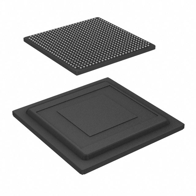
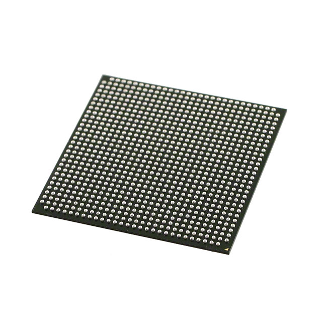
The 5AGXBA3D4F27I5N is an Arria V GX-family FPGA IC designed for applications that require substantial on-chip logic capacity and embedded RAM. This device provides 156,000 logic elements and 11,746,304 total RAM bits in a surface-mount 672-ball FCBGA package, delivering a compact, high-density programmable fabric for system designers.
With 336 I/O pins, an industrial operating temperature range, and a tightly specified core supply window, this FPGA targets industrial and embedded designs that need large logic resources, substantial on-chip memory, and robust environmental tolerance.
Key Features
- Core Logic 156,000 logic elements provide significant programmable logic capacity for complex digital functions and custom accelerators.
- On‑chip Memory 11,746,304 total RAM bits enable large user memory space for buffers, FIFOs, and temporary storage without external memory dependence.
- I/O Density 336 general-purpose I/O pins support extensive peripheral interfacing and multi-channel connectivity in a single device.
- Power Supply Core voltage supply specified at 1.07 V to 1.13 V for precise power planning and regulator selection.
- Package & Mounting 672-ball BGA (FCBGA) package, supplier package 672-FBGA (27×27), optimized for surface-mount assembly and dense board layouts.
- Industrial Grade & Temperature Range Rated industrial grade with operating temperature from −40 °C to 100 °C for deployment in demanding environments.
- RoHS Compliant Meets RoHS environmental requirements for use in modern manufacturing processes.
Typical Applications
- Industrial Control Programmable control logic, custom I/O handling, and embedded protocol bridging where industrial temperature range and high logic density are required.
- Communications & Networking Protocol processing, packet buffering, and interface aggregation using extensive I/O and large on‑chip RAM resources.
- Video and Image Processing Real‑time processing pipelines and frame buffering leveraging the device's logic capacity and substantial RAM bits.
- Embedded Acceleration Hardware acceleration for compute‑intensive tasks that benefit from large programmable fabric and local memory.
Unique Advantages
- High logic capacity: 156,000 logic elements support complex, large-scale designs without immediate partitioning across multiple devices.
- Large on‑chip RAM: 11,746,304 RAM bits reduce reliance on external memory, improving latency and simplifying board-level BOM.
- Extensive I/O: 336 I/O pins enable multi‑channel interfacing and flexible system partitioning in one FPGA.
- Industrial reliability: Rated for −40 °C to 100 °C operation to meet the environmental demands of industrial deployments.
- Compact, assembly-friendly package: 672-ball FCBGA (27×27) package supports dense PCB integration while remaining compatible with standard surface-mount assembly processes.
- Predictable power planning: Narrow core supply window (1.07–1.13 V) simplifies regulator selection and power‑domain design.
Why Choose 5AGXBA3D4F27I5N?
The 5AGXBA3D4F27I5N Arria V GX FPGA combines a high count of logic elements, substantial embedded RAM, and a broad I/O complement in a single industrial‑grade FCBGA package. This combination is well suited to embedded and industrial systems that require on-chip resources to implement complex logic, buffering, and interface aggregation without escalating board complexity.
Engineers specifying this device can expect a compact, high-density programmable solution that supports robust thermal and voltage environments, simplifying system architecture while providing headroom for feature growth and iterative hardware acceleration development.
Request a quote or submit a pricing inquiry for 5AGXBA3D4F27I5N through your preferred procurement channel to obtain availability and lead‑time information.


Date Founded: 1968
Headquarters: Santa Clara, California, USA
Employees: 130,000+
Revenue: $54.23 Billion
Certifications and Memberships: ISO9001:2015, ISO14001:2015, ISO17025:2017, ISO27001:2022, ISO45001:2018, ISO50001:2018


