
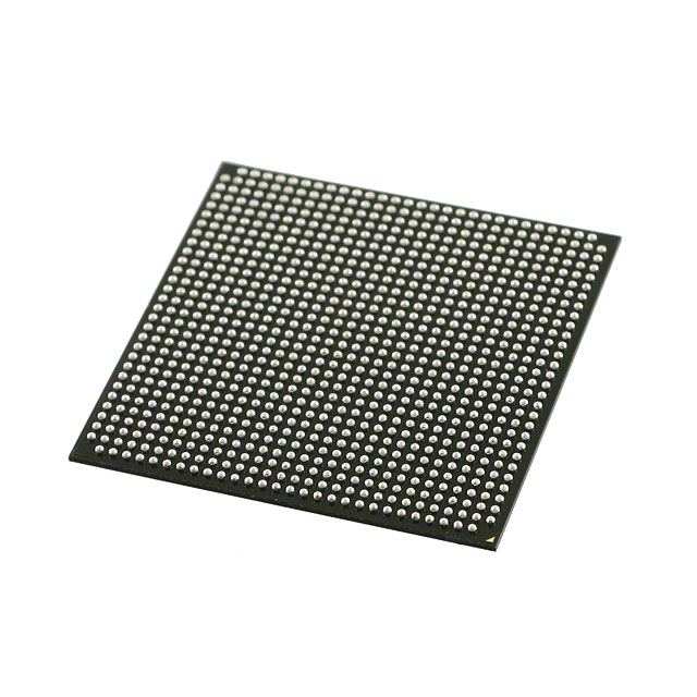
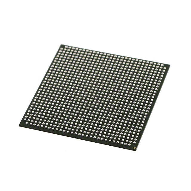
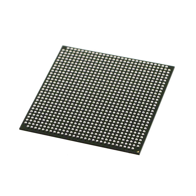
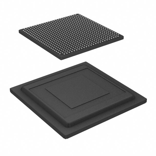
5AGXBA3D4F31C4N
| Part Description |
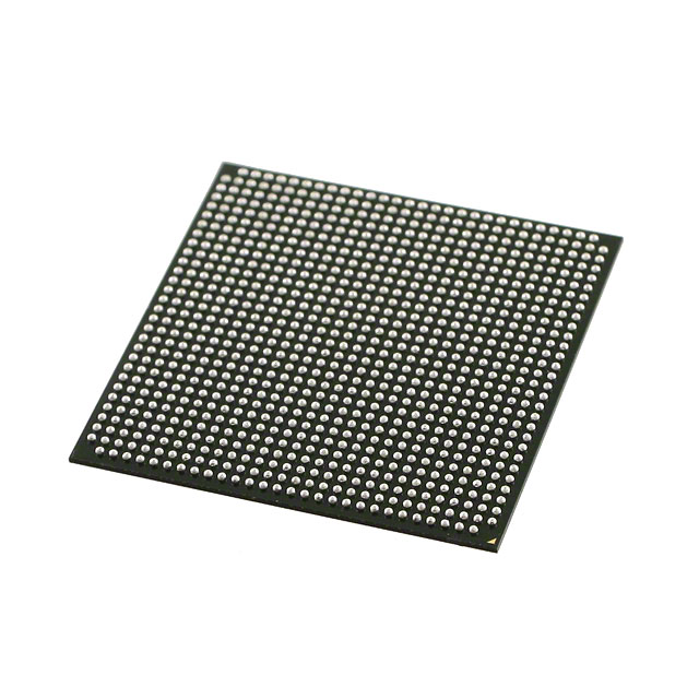
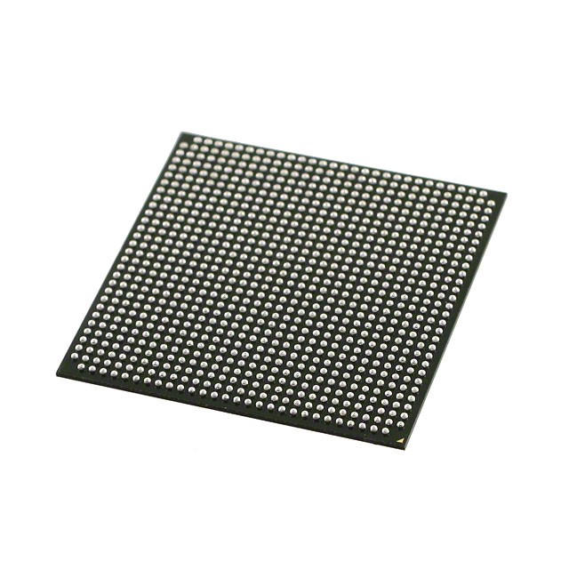
Arria V GX Field Programmable Gate Array (FPGA) IC 416 11746304 156000 896-BBGA, FCBGA |
|---|---|
| Quantity | 240 Available (as of October 8, 2026) |
| Product Category | Field Programmable Gate Array (FPGA) |
|---|---|
| Manufacturer | Intel |
| Manufacturing Status | Obsolete |
| Manufacturer Standard Lead Time | Contact Us |
| Datasheet |
Specifications & Environmental
| Device Package | 896-FBGA (31x31) | Grade | Commercial | Operating Temperature | 0°C – 85°C | ||
|---|---|---|---|---|---|---|---|
| Package / Case | 896-BBGA, FCBGA | Number of I/O | 416 | Voltage | 1.07 V - 1.13 V | ||
| Mounting Method | Surface Mount | RoHS Compliance | RoHS Compliant | REACH Compliance | REACH Unknown | ||
| Moisture Sensitivity Level | 3 (168 Hours) | Number of LABs/CLBs | 7362 | Number of Logic Elements/Cells | 156000 | ||
| Number of Gates | N/A | ECCN | 3A001A2C | HTS Code | 8542.39.0001 | ||
| Qualification | N/A | Total RAM Bits | 11746304 |
Overview of 5AGXBA3D4F31C4N – Arria V GX Field Programmable Gate Array (FPGA) IC 416 11746304 156000 896-BBGA, FCBGA
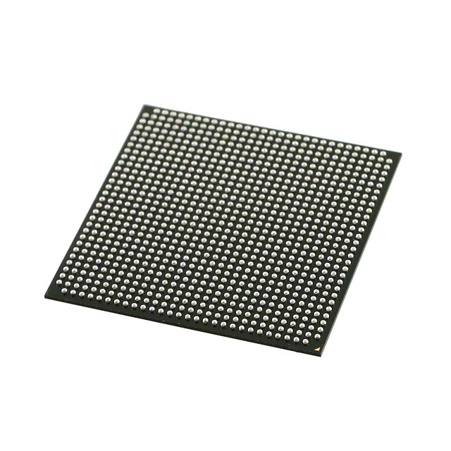
The 5AGXBA3D4F31C4N is an Intel Arria V GX field programmable gate array (FPGA) supplied in a 896‑BBGA FCBGA surface‑mount package (896‑FBGA, 31×31). It is offered in a commercial grade device designed for applications that require dense programmable logic, significant on‑chip RAM, and extensive I/O connectivity.
Key device attributes include 156,000 logic elements, 11,746,304 total RAM bits, 416 I/O pins, a nominal core supply range of 1.07 V to 1.13 V, and an operating temperature range of 0 °C to 85 °C. The component is RoHS‑compliant and is supported by Arria V‑series documentation covering electrical, switching, configuration, and I/O timing characteristics.
Key Features
- Logic Capacity — 156,000 logic elements provide high-density programmable logic for complex designs and parallel processing.
- On‑Chip Memory — 11,746,304 total RAM bits for buffering, local storage, and memory‑intensive logic functions.
- I/O Resources — 416 I/O pins to support broad peripheral interfacing and multi‑channel signal routing.
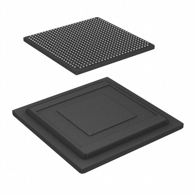
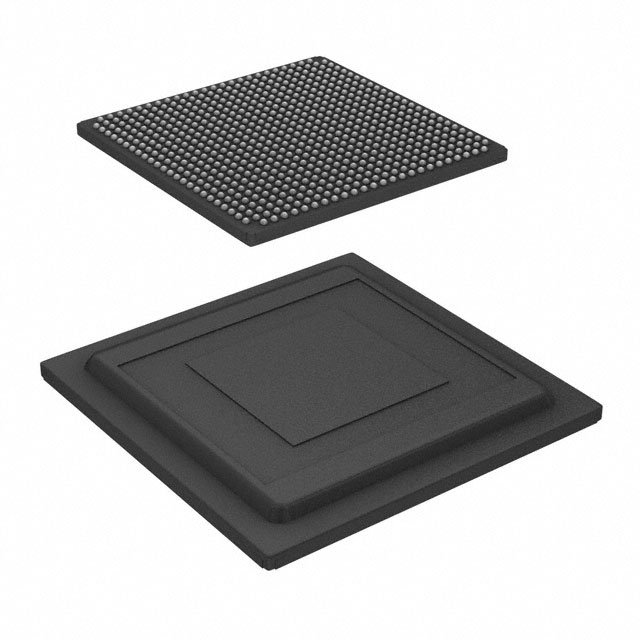
- Package and Mounting — 896‑BBGA FCBGA package (896‑FBGA, 31×31) designed for surface‑mount PCB assembly in compact layouts.
- Power — Core voltage supply specified from 1.07 V to 1.13 V to match system power domains.
- Operating Conditions — Commercial grade device rated for 0 °C to 85 °C operation, suitable for standard commercial environments.
- Regulatory — RoHS‑compliant for environmentally conscious manufacturing and regulatory alignment.
- Series Documentation — Arria V device datasheet coverage includes electrical characteristics, switching characteristics, configuration specifications, and I/O timing for the Arria V family.
Typical Applications
- High‑density signal processing — Implement compute‑heavy logic and parallel processing tasks using 156,000 logic elements and large on‑chip RAM.
- Communications and transceiver systems — Designs that require extensive I/O connectivity and series‑level transceiver specifications documented for Arria V devices.
- Embedded compute and prototyping — Platform development and proof‑of‑concept systems that benefit from reprogrammable logic and abundant memory resources.
- Custom accelerators — Offload algorithmic or pipeline stages to FPGA fabric using the device’s logic capacity and RAM resources.
Unique Advantages
- High logic and memory density: 156,000 logic elements combined with over 11.7 million RAM bits enable complex designs without immediate external memory dependence.
- Extensive I/O count: 416 I/O pins allow flexible system interfacing and multi‑channel connectivity in a single device.
- Compact FCBGA packaging: 896‑BBGA (31×31) footprint supports compact board designs while preserving high pin count.
- Predictable power domain: Narrow core supply range (1.07 V–1.13 V) simplifies power budgeting and supply design.
- Commercial availability and compliance: Commercial grade part with RoHS compliance for mainstream product and development use.
- Documented device family support: Arria V series datasheet material provides detailed electrical, switching, configuration, and I/O timing guidance for design and integration.
Why Choose 5AGXBA3D4F31C4N?
The 5AGXBA3D4F31C4N positions itself as a high‑density, commercially graded Arria V GX FPGA option for designs that need substantial programmable logic, on‑chip RAM, and broad I/O within a compact BGA package. Its documented operating conditions and series‑level datasheet coverage help engineers assess electrical and timing behavior during integration.
This device is well suited for engineering teams developing complex digital systems, communications interfaces, and prototype platforms that require reconfigurable logic capacity, significant memory resources, and predictable power and thermal envelopes in commercial environments.
Request a quote or submit a procurement inquiry to receive availability and pricing information for 5AGXBA3D4F31C4N. Our team can provide component lead times and support materials to assist your design and sourcing process.





















Date Founded: 1968
Headquarters: Santa Clara, California, USA
Employees: 130,000+
Revenue: $54.23 Billion
Certifications and Memberships: ISO9001:2015, ISO14001:2015, ISO17025:2017, ISO27001:2022, ISO45001:2018, ISO50001:2018


