
5AGXBA1D6F31C6G
| Part Description |
Arria V GX Field Programmable Gate Array (FPGA) IC 384 8666112 75000 896-BBGA, FCBGA |
|---|---|
| Quantity | 1,733 Available (as of June 15, 2026) |

| Product Category | Field Programmable Gate Array (FPGA) |
|---|---|
| Manufacturer | Intel |
| Manufacturing Status | Active |
| Manufacturer Standard Lead Time | 16 Weeks |
| Datasheet |
Specifications & Environmental
| Device Package | 896-FBGA (31x31) | Grade | Commercial | Operating Temperature | 0°C – 85°C | ||
|---|---|---|---|---|---|---|---|
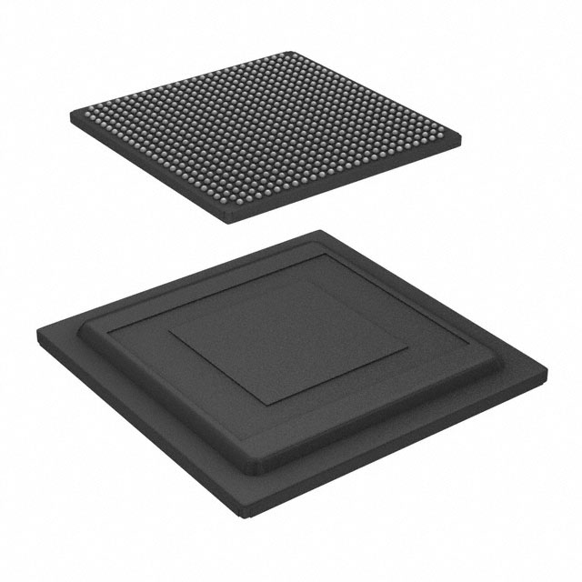
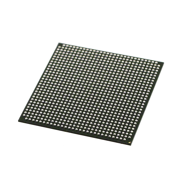
| Package / Case | 896-BBGA, FCBGA | Number of I/O | 384 | Voltage | 1.07 V - 1.13 V | ||
| Mounting Method | Surface Mount | RoHS Compliance | RoHS Compliant | REACH Compliance | REACH Unaffected | ||
| Moisture Sensitivity Level | 3 (168 Hours) | Number of LABs/CLBs | 3537 | Number of Logic Elements/Cells | 75000 | ||
| Number of Gates | N/A | ECCN | PENDING ECCN | HTS Code | 0000.00.0000 | ||
| Qualification | N/A | Total RAM Bits | 8666112 |
Overview of 5AGXBA1D6F31C6G – Arria V GX Field Programmable Gate Array (FPGA) IC, 896-BBGA FCBGA
The 5AGXBA1D6F31C6G is an Arria V GX family Field Programmable Gate Array (FPGA) supplied in a 896-BBGA (896-FBGA, 31×31) surface-mount package. It offers a combination of on-chip programmable logic, embedded RAM, and extensive I/O for complex digital designs that require substantial logic density and memory resources.
This commercial-grade device is suitable for designs that need high logic capacity, significant on-chip RAM, and a large number of I/O signals while operating within a defined core voltage range and a commercial temperature window.
Key Features
- Programmable Logic Capacity — 75,000 logic elements to implement complex custom logic, state machines, and digital processing functions.
- Embedded Memory — 8,666,112 total RAM bits available on-chip for FIFOs, buffers, and local data storage.
- Rich I/O — 384 user I/O pins to support broad connectivity and interfacing requirements in dense systems.
- Package & Mounting — 896-BBGA (FCBGA) 31×31 supplier device package in a surface-mount form factor for board-level integration.
- Power Supply — Core supply voltage specified between 1.07 V and 1.13 V for predictable power design and sequencing.
- Operating Range — Commercial-grade operating temperature range from 0 °C to 85 °C.
- Standards Compliance — RoHS-compliant for environmental regulatory conformity.
- Comprehensive Documentation — Supported by the Arria V device datasheet, which details electrical characteristics, configuration timing, and I/O timing for Arria V devices.
Typical Applications
- High-density digital processing — Use the 75,000 logic elements and large embedded RAM to implement complex signal processing, algorithm acceleration, or custom datapaths.
- Board-level system integration — The 384 I/O pins and compact 896-BBGA package enable dense interfacing and routing for multifunction boards and modules.
- Prototyping and custom SoC glue logic — Leverage programmable logic and on-chip memory to prototype custom interfaces and integrate peripheral logic without adding discrete components.
Unique Advantages
- High logic density: 75,000 logic elements provide capacity for complex designs and partitioning of functions on a single device.
- Large on-chip RAM: 8,666,112 total RAM bits reduce external memory dependency for buffer and local data storage.
- Extensive I/O count: 384 I/Os enable broad connectivity to peripherals, high-pin-count connectors, and multi-channel interfaces.
- Compact surface-mount package: 896-BBGA (31×31) balances board area and I/O density for space-constrained designs.
- Defined power window: Narrow core voltage range (1.07–1.13 V) simplifies power-supply selection and sequencing design constraints.
- Regulatory compliance: RoHS-compliant device suitable for markets requiring lead-free components.
Why Choose 5AGXBA1D6F31C6G?
The 5AGXBA1D6F31C6G Arria V GX FPGA delivers a balanced combination of logic capacity, embedded RAM, and I/O resources in a commercially rated, surface-mount 896-BBGA package. Its specifications—75,000 logic elements, over 8.6 million RAM bits, and 384 I/Os—make it well suited for designs that require substantial on-chip resources and dense interfacing within a commercial temperature range.
Engineers and procurement teams can rely on the Arria V device documentation for detailed electrical and configuration guidance, enabling informed integration and reliable system-level design choices for medium- to high-complexity FPGA applications.
Request a quote or submit a product inquiry to receive pricing and availability for the 5AGXBA1D6F31C6G Arria V GX FPGA.


Date Founded: 1968
Headquarters: Santa Clara, California, USA
Employees: 130,000+
Revenue: $54.23 Billion
Certifications and Memberships: ISO9001:2015, ISO14001:2015, ISO17025:2017, ISO27001:2022, ISO45001:2018, ISO50001:2018


