
5AGXBA1D6F31C6N
| Part Description |
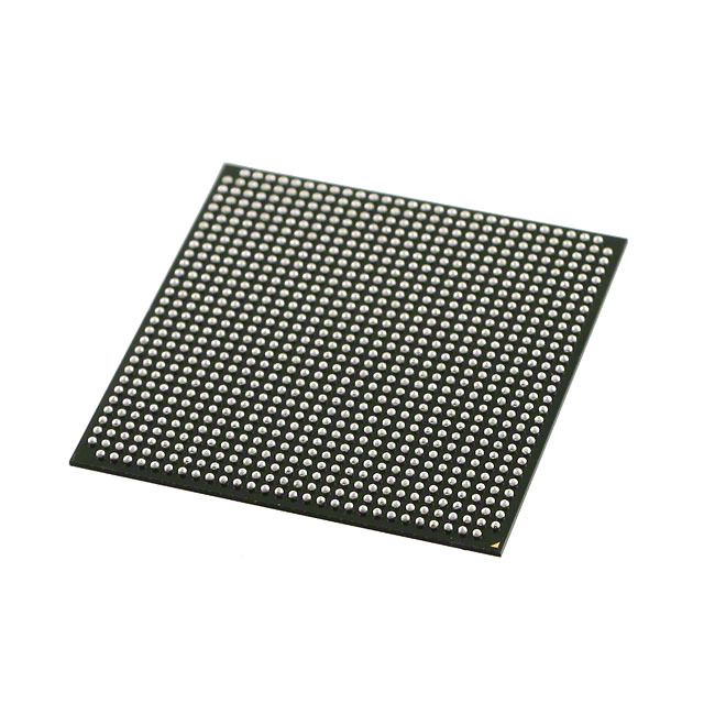
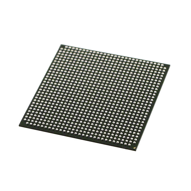
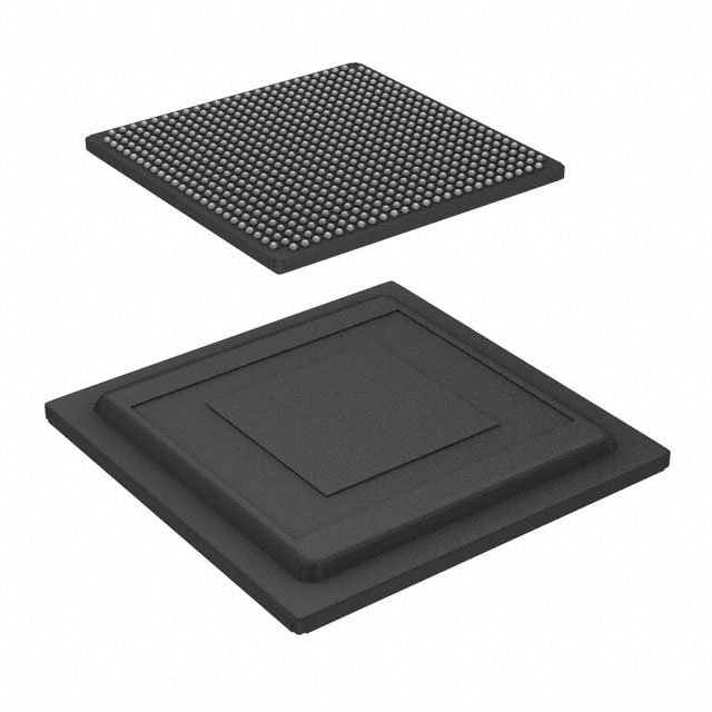
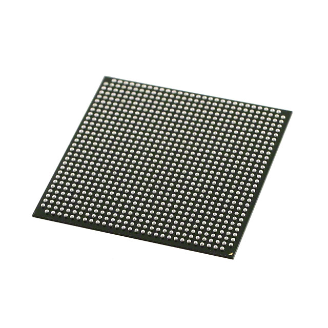
Arria V GX Field Programmable Gate Array (FPGA) IC 416 8666112 75000 896-BBGA, FCBGA |
|---|---|
| Quantity | 744 Available (as of October 7, 2026) |
| Product Category | Field Programmable Gate Array (FPGA) |
|---|---|
| Manufacturer | Intel |
| Manufacturing Status | Obsolete |
| Manufacturer Standard Lead Time | Contact Us |
| Datasheet |
Specifications & Environmental
| Device Package | 896-FBGA (31x31) | Grade | Commercial | Operating Temperature | 0°C – 85°C | ||
|---|---|---|---|---|---|---|---|
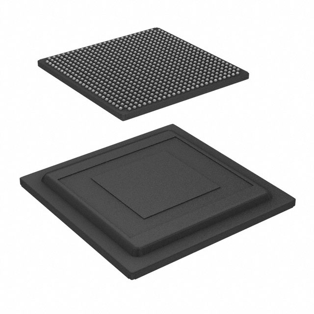
| Package / Case | 896-BBGA, FCBGA | Number of I/O | 416 | Voltage | 1.07 V - 1.13 V | ||
| Mounting Method | Surface Mount | RoHS Compliance | RoHS Compliant | REACH Compliance | REACH Unknown | ||
| Moisture Sensitivity Level | 3 (168 Hours) | Number of LABs/CLBs | 3537 | Number of Logic Elements/Cells | 75000 | ||
| Number of Gates | N/A | ECCN | 3A001A2C | HTS Code | 8542.39.0001 | ||
| Qualification | N/A | Total RAM Bits | 8666112 |
Overview of 5AGXBA1D6F31C6N – Arria V GX FPGA, 75,000 Logic Elements, 896‑BBGA FCBGA
The 5AGXBA1D6F31C6N is an Intel Arria V GX field‑programmable gate array (FPGA) supplied in an 896‑BBGA FCBGA package. It delivers up to 75,000 logic elements with 8,666,112 total on‑chip RAM bits and 416 user I/O pins for high‑density programmable logic designs.
Designed for commercial‑grade applications, this device targets designs that require substantial logic density, significant embedded memory, and a large I/O complement while operating within a 1.07 V to 1.13 V core supply range and a 0 °C to 85 °C operating temperature window.
Key Features
- Core Logic Approximately 75,000 logic elements to implement complex digital functions and custom processing pipelines.
- On‑Chip RAM 8,666,112 total RAM bits of embedded memory for buffers, FIFOs, and local data storage without external memory.
- I/O Capacity 416 user I/O pins provide extensive interface options for sensors, peripherals, and board‑level interconnects.
- Package and Mounting 896‑ball BGA (FCBGA) package, supplier device package 896‑FBGA (31×31), optimized for surface‑mount assembly.
- Power and Operating Conditions Core voltage specified between 1.07 V and 1.13 V; commercial operating temperature range of 0 °C to 85 °C.
- Regulatory Compliance RoHS‑compliant component suitable for designs requiring lead‑free, environmentally compliant parts.
- Documentation Detailed Arria V device datasheet available covering electrical characteristics, switching characteristics, configuration specifications, and I/O timing.
Typical Applications
- Custom Logic Acceleration Implement hardware acceleration and datapath logic using the device’s 75,000 logic elements and extensive on‑chip RAM.
- High‑Density I/O Systems Drive complex multi‑channel interfaces and board I/O requirements with 416 available I/O pins.
- Embedded Memory‑Centric Designs Use the large embedded RAM array for packet buffering, frame storage, or algorithm state memory without external DRAM.
Unique Advantages
- High Logic Density: 75,000 logic elements enable substantial integration of combinational and sequential logic on a single device, reducing component count.
- Large On‑Chip Memory: Over 8.6 million RAM bits provide significant local storage for latency-sensitive data and pipeline buffering.
- Extensive I/O: 416 I/Os support multiple parallel interfaces and flexible board routing for complex system designs.
- Compact BGA Package: The 896‑ball FCBGA (31×31) package offers a dense footprint for space‑constrained boards while supporting surface‑mount assembly.
- Commercial‑Grade Reliability: Rated for 0 °C to 85 °C operation and RoHS compliance for mainstream commercial applications.
- Tightly Defined Power Envelope: Narrow core voltage range (1.07 V–1.13 V) simplifies power‑rail design and control for consistent device behavior.
Why Choose 5AGXBA1D6F31C6N?
The 5AGXBA1D6F31C6N Arria V GX FPGA combines substantial logic capacity, a large embedded RAM resource, and a high I/O count in a single 896‑BBGA package, making it well suited to commercial designs that demand integrated programmable logic and on‑chip memory. Its defined operating voltage and temperature range, together with RoHS compliance and comprehensive datasheet coverage, help accelerate design validation and deployment.
This device is a practical option for engineering teams building mid‑to‑high complexity FPGA designs that require high logic density, sizable local memory, and broad interfacing capability within a commercial‑grade product envelope.
Request a quote or submit an inquiry to receive pricing, availability, and additional integration information for 5AGXBA1D6F31C6N.





















Date Founded: 1968
Headquarters: Santa Clara, California, USA
Employees: 130,000+
Revenue: $54.23 Billion
Certifications and Memberships: ISO9001:2015, ISO14001:2015, ISO17025:2017, ISO27001:2022, ISO45001:2018, ISO50001:2018


