
5AGXBA5D4F27C4N
| Part Description |
Arria V GX Field Programmable Gate Array (FPGA) IC 336 13284352 190000 672-BBGA, FCBGA |
|---|---|
| Quantity | 210 Available (as of June 15, 2026) |

| Product Category | Field Programmable Gate Array (FPGA) |
|---|---|
| Manufacturer | Intel |
| Manufacturing Status | Obsolete |
| Manufacturer Standard Lead Time | Contact Us |
| Datasheet |
Specifications & Environmental
| Device Package | 672-FBGA (27x27) | Grade | Commercial | Operating Temperature | 0°C – 85°C | ||
|---|---|---|---|---|---|---|---|
| Package / Case | 672-BBGA, FCBGA | Number of I/O | 336 | Voltage | 1.07 V - 1.13 V | ||
| Mounting Method | Surface Mount | RoHS Compliance | RoHS Compliant | REACH Compliance | REACH Unknown | ||
| Moisture Sensitivity Level | 3 (168 Hours) | Number of LABs/CLBs | 8962 | Number of Logic Elements/Cells | 190000 | ||
| Number of Gates | N/A | ECCN | 3A001A2C | HTS Code | 8542.39.0001 | ||
| Qualification | N/A | Total RAM Bits | 13284352 |
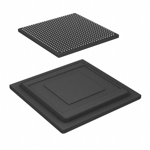
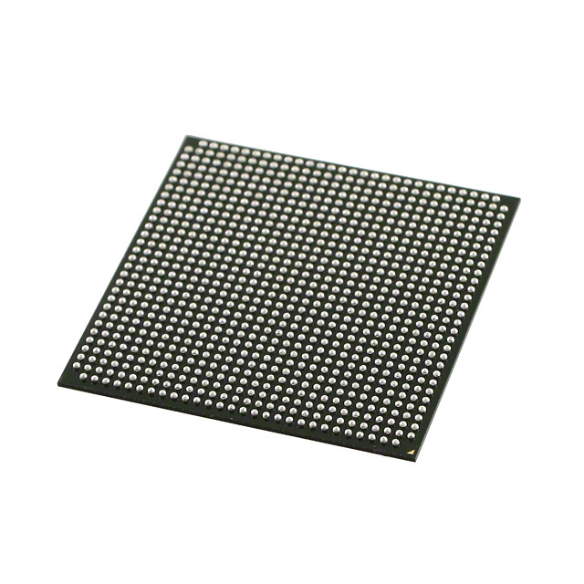
Overview of 5AGXBA5D4F27C4N – Arria V GX FPGA — 190,000 logic elements, 336 I/Os, 672‑BBGA
The 5AGXBA5D4F27C4N is an Arria V GX Field Programmable Gate Array (FPGA) in a 672‑BBGA FCBGA package designed for commercial-grade applications. The device provides a high density of programmable logic and on‑chip RAM, with a defined operating voltage range and temperature rating suitable for standard embedded and electronic system designs.
Key device attributes include 190,000 logic elements, 13,284,352 total RAM bits, 336 user I/O pins, surface‑mount 672‑FBGA (27×27) package, and RoHS compliance—specifications that support complex, high‑density digital implementations.
Key Features
- Core Logic — 190,000 logic elements to implement large-scale custom digital functions and control logic.
- On‑Chip Memory — 13,284,352 total RAM bits for embedded data storage, buffering, and state machines.
- I/O Count — 336 I/O pins for broad external interfacing and multi‑bus connectivity.
- Package & Mounting — 672‑BBGA (FCBGA) supplier package (672‑FBGA, 27×27) with surface‑mount assembly suitable for compact board layouts.
- Power — Core supply specified at 1.07 V to 1.13 V for power rail planning and system design.
- Temperature & Grade — Commercial grade with an operating temperature range of 0 °C to 85 °C.
- Compliance — RoHS compliant to support regulatory and environmental requirements.
Typical Applications
- Custom digital logic — Implement complex, application‑specific logic using 190,000 logic elements and extensive on‑chip RAM for state, buffering, and algorithm implementation.
- High‑I/O interface designs — Leverage 336 I/O pins for multi‑channel interfacing, protocol bridging, and peripheral integration on compact PCBs.
- Embedded system integration — Use the commercial‑grade Arria V GX device in embedded products that require substantial programmable logic and memory resources within a 672‑BBGA package.
Unique Advantages
- High logic density: 190,000 logic elements provide extensive capacity for large designs without immediate migration to larger device families.
- Significant on‑chip RAM: 13,284,352 total RAM bits reduce external memory dependence for many buffering and storage needs, simplifying BOM and board routing.
- Generous I/O count: 336 I/Os enable flexible system partitioning and support for multiple interfaces on a single device.
- Compact package: 672‑FBGA (27×27) footprint delivers high integration density in a surface‑mount form factor suitable for space‑constrained designs.
- Clear power envelope: Defined core supply range of 1.07 V to 1.13 V helps streamline power‑rail design and verification.
- Regulatory readiness: RoHS compliance supports inclusion in environmentally regulated products and assemblies.
Why Choose 5AGXBA5D4F27C4N?
The 5AGXBA5D4F27C4N Arria V GX FPGA positions itself as a high‑density, commercially rated programmable logic device for designs that require substantial logic resources, on‑chip memory, and a high number of I/Os in a compact BGA package. The combination of 190,000 logic elements and over 13 million RAM bits makes it suitable for designs where integration and on‑chip memory reduce external component count and simplify board architecture.
This device is appropriate for engineering teams developing embedded systems and digital logic applications that operate within a 0 °C to 85 °C commercial range and a defined core voltage window. Its RoHS compliance and well‑specified electrical and package characteristics support repeatable manufacturing and system integration.
Request a quote or submit a purchasing inquiry to obtain pricing, availability, and ordering information for the 5AGXBA5D4F27C4N Arria V GX FPGA.


Date Founded: 1968
Headquarters: Santa Clara, California, USA
Employees: 130,000+
Revenue: $54.23 Billion
Certifications and Memberships: ISO9001:2015, ISO14001:2015, ISO17025:2017, ISO27001:2022, ISO45001:2018, ISO50001:2018


